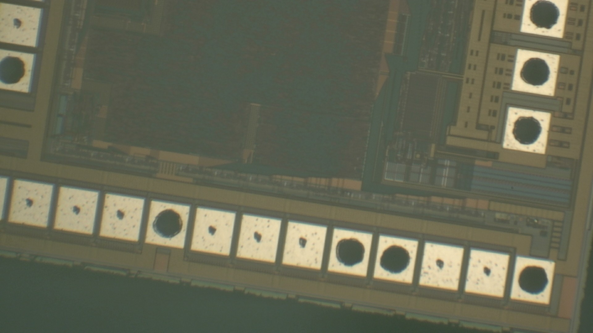
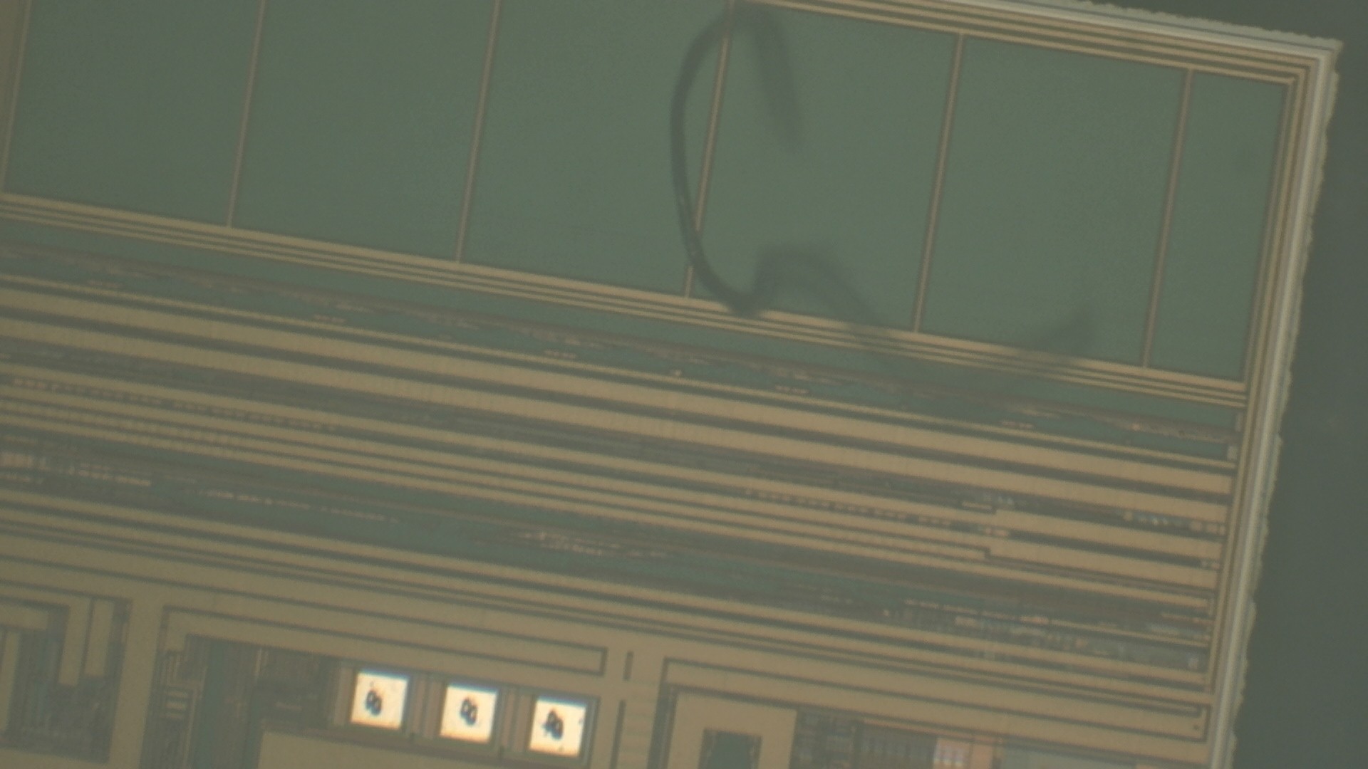
 Microprocessor PIC18F4510 Eeprom Memory Breaking
Protective microprocessor PIC18F4510 eeprom data memory and flash program memory breaking needs to crack secured MICROCHIP MCU PIC18F4510 fuse bit, unlock microcontroller PIC18F4510 and readout embedded firmware in the format of binary file or heximal data;
While the use of the BSR with an embedded 8-bit address allows users to address the entire range of data memory which can facilitate Microprocessor PIC18F4510 Eeprom Memory Breaking, it also means that the user must always ensure that the correct bank is selected. Otherwise, data may be read from or written to the wrong location.
la memoria dati eeprom del microprocessore protettivo PIC18F4510 e la rottura della memoria del programma flash necessitano di crack protetti, bit fusibile MICROCHIP MCU PIC18F4510, sblocco del microcontrollore PIC18F4510 e lettura del firmware incorporato nel formato di file binario o dati essimali;
This can be disastrous if a GPR is the intended target of an operation, but an SFR is written to instead. Verifying and/or changing the BSR for each read or write to data memory can become very inefficient.
To streamline access for the most commonly used data memory locations, the data memory is configured with an Access Bank, which allows users to access a mapped block of memory without specifying a BSR. The Access Bank consists of the first 128 bytes of memory (00h-7Fh) in Bank 0 and the last 128 bytes of memory (80h-FFh) in Block 15.
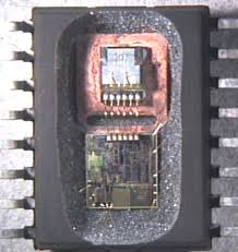
Microprocessor PIC18F4510 Eeprom Memory Breaking
The lower half is known as the “Access RAM” and is composed of GPRs. This upper half is also where the device’s SFRs are mapped. These two areas are mapped contiguously in the Access Bank and can be addressed in a linear fashion by an 8-bit address.

koruyucu mikroişlemci PIC18F4510 eeprom veri belleği ve flash program belleği kırma, güvenli MICROCHIP MCU PIC18F4510 sigorta bitini kırmalı, mikrodenetleyici PIC18F4510’un kilidini açmalı ve yerleşik bellenimi ikili dosya veya onaltılı veri formatında okumalıdır;
The Access Bank is used by core PIC18F4510 instructions that include the Access RAM bit (the ‘a’ parameter in the instruction). When ‘a’ is equal to ‘1’, the instruction uses the BSR and the 8-bit address included in the opcode for the data memory address. When ‘a’ is ‘0’,
védő mikroprocesszor PIC18F4510 eeprom adatmemória és flash program memória feltörése fel kell törni a biztonságos MICROCHIP MCU PIC18F4510 biztosítékbitet, fel kell oldani a PIC18F4510 mikrovezérlőt és ki kell olvasni a beágyazott firmware-t bináris fájl vagy heximális adat formátumban;