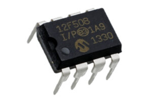
Microchip PIC12F508 Processor Flash Memory Breaking will disable the protection over the flash memory, original embedded firmware will be read through programmer;

Przerwanie pamięci flash procesora Microchip PIC12F508 spowoduje wyłączenie ochrony pamięci flash, oryginalne wbudowane oprogramowanie sprzętowe zostanie odczytane przez programator
If the low-power mode clock frequency is less than 1 MHz, the A/D RC clock source should be selected. Operation in the Low-Power Sleep mode requires the A/ D RC clock to be selected. If bits, ACQT2:ACQT0, are set to ‘000’ and a conversion is started, the conversion will be delayed one instruction cycle to allow execution of the SLEEP instruction and entry to Low-Power Sleep mode by recovering pic12f508 mcu source code. The IDLEN and SCS bits in the OSCCON register must have already been cleared prior to starting the conversion.
The ADCON1, TRISA and TRISB registers all configure the A/D port pins. The port pins needed as analog inputs must have their corresponding TRIS bits set (input). If the TRIS bit is cleared (output), the digital output level (VOH or VOL) will be converted. The A/D operation is independent of the state of the CHS2:CHS0 bits and the TRIS bits.

Mikrokontroler Microchip PIC12F508 łamie i wyodrębnia plik szesnastkowy z jego pamięci flash i pamięci eeprom,
When reading the Port register, all pins configured as analog input channels will read as cleared (a low level). Pins con- figured as digital inputs will convert an analog input. Analog levels on a digitally configured input will be accurately converted to decrypt locked chip pic12f508 firmware from its flash memory.
Analog levels on any pin defined as a digital input may cause the digital input buffer to consume current out of the device’s specification limits.
