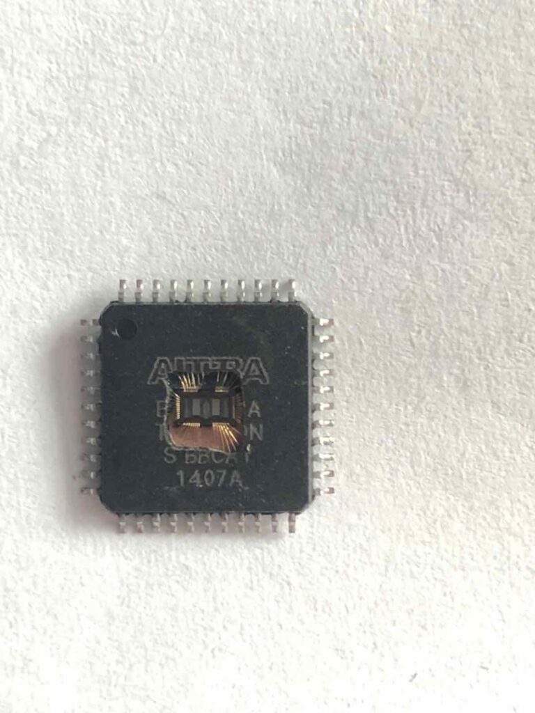
 Freescale Encrypted MCU SPC5602DF1VLH4R Flash Data Cloning
Freescale Encrypted MCU SPC5602DF1VLH4R Flash Data Cloning means the embedded firmware from original Microcontroller spc5602df1 will be unlocked and extract the binary file directly from opened microprocessor;

The device provides four main I/O pad types depending on the associated alternate functions:
Slow pads—These pads are the most common pads, providing a good compromise between transition time and low electromagnetic emission.
Medium pads—These pads provide transition fast enough for the serial communication channels with controlled current to reduce electromagnetic emission when copying spc5602pef0m1 secured mcu flash binary.
Input only pads—These pads are associated to ADC channels (ADC_P[X]) providing low input leakage.
Medium pads can use slow configuration to reduce electromagnetic emission except for PC[1], that is medium only, at the cost of reducing AC performance in order to reading out spc5601df1m1 microcontroller flash content.
TABLE : I/O input DC electrical characteristics
| Symbol | C | Parameter | Conditions1 | Value | Unit | ||||
| Min | Typ | Max | |||||||
| VIH | SR | P | Input high level CMOS (Schmitt Trigger) | — | 0.65VDD | — | VDD+0.4 | V | |
| VIL | SR | P | Input low level CMOS (Schmitt Trigger) | — | -0.4 | — | 0.35VDD | V | |
| VHYS | CC | C | Input hysteresis CMOS (Schmitt Trigger) | — | 0.1VDD | — | — | V | |
| ILKG | CC | D | Digital input leakage | No injection on adjacent pin | TA = -40 °C | — | 2 | 200 | nA |
| D | TA = 25 °C | — | 2 | 200 | |||||
| D | TA = 85 °C | — | 5 | 300 | |||||
| D | TA = 105 °C | — | 12 | 500 | |||||
| P | TA = 125 °C | — | 70 | 1000 | |||||
| WFI2 | SR | P | Digital input filtered pulse | — | — | — | 40 | ns | |
| (2) WNFI | SR | P | Digital input not filtered pulse | — | 1000 | — | — | ns |
VDD = 3.3 V ± 10% / 5.0 V ± 10%, TA = -40 to 125 °C, unless otherwise specified
2 In the range from 40 to 1000 ns, pulses can be filtered or not filtered, according to operating temperature and voltage.
| Symbol | C | Parameter | Conditions1 | Value | Unit | ||||
| Min | Typ | Max | |||||||
| |IWPU| | CC | P | Weak pull-up current absolute value | VIN = VIL, VDD = 5.0 V ± 10% | PAD3V5V = 0 | 10 | — | 150 | µA |
| C | PAD3V5V = 12 | 10 | — | 250 | |||||
| P | VIN = VIL, VDD = 3.3 V ± 10% | PAD3V5V = 1 | 10 | — | 150 | ||||
| |IWPD| | CC | P | Weak pull-down current absolute value | VIN = VIH, VDD = 5.0 V ± 10% | PAD3V5V = 0 | 10 | — | 150 | µA |
| C | PAD3V5V = 1(2) | 10 | — | 250 | |||||
| P | VIN = VIH, VDD = 3.3 V ± 10% | PAD3V5V = 1 | 10 | — | 150 |
- VDD = 3.3 V ± 10% / 5.0 V ± 10%, TA = -40 to 125 °C, unless otherwise specified.
- 2 The configuration PAD3V5 = 1 when VDD = 5 V is only a transient configuration during power-up. All pads but RESET are configured in input or in high impedance state.