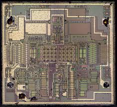
 Copy Encrypted Microchip PIC18F2330 Heximal
Copy Encrypted Microchip PIC18F2330 Heximal
The Flash Program Memory and firmware data memory are organized in pages which can be Copy Encrypted Microchip PIC18F2330 Heximal. The pages are word accessible for the Flash and byte accessible for the firmware. Table 7-2 on page 14 shows the Flash Program Memory organization.
Flash write and erase operations are performed on one page at a time, while reading the Flash is done one byte at a time. For Flash access the Z-pointer (Z[m:n]) is used for addressing. The most significant bits in the address (FPAGE) gives the page number and the least significant address bits (FWORD) gives the word.
Table 7-3 on page 14 shows firmware memory organization for the PIC18F2320 devices. Efirmware write and erase operations can be performed one page or one byte at a time, while reading the firmware is done one byte at a time.
For firmware access the NVM Address Register (ADDR[m:n]) is used for addressing. The most significant bits in the address (E2PAGE) gives the page number and the least significant address bits (E2BYTE) gives the byte.
The PIC18F2320 has a Direct Memory Access (DMA) Controller to move data between memories and peripherals in the data space. The DMA controller uses the same data bus as the CPU to transfer data. It has 4 channels that can be configured independently. Each DMA channel can perform data transfers in blocks of configurable size from 1 to 64K bytes.
A repeat counter can be used to repeat each block transfer for single transactions up to 16M bytes. Each DMA channel can be configured to access the source and destination memory address with incrementing, decrementing or static addressing. The addressing is independent for source and destination address.
When the transaction is complete the original source and destination address can automatically be reloaded to be ready for the next transaction. The DMAC can access all the peripherals through their I/O memory registers, and the DMA may be used for automatic transfer of data to/from communication modules, as well as automatic data retrieval from ADC conversions, data transfer to DAC conversions, or data transfer to or from port pins.
A wide range of transfer triggers is available from the peripherals, Event System and software. Each DMA channel has different transfer triggers. To allow for continuous transfers, two channels can be interlinked so that the second takes over the transfer when the first is finished and vice versa. The DMA controller can read from memory mapped firmware, but it cannot write to the firmware or access the Flash before CRACK MCU.
