Archive for the ‘Reverse Engineer Microcontroller’ Category
 Reverse Engineering Microcontroller PIC12C509A Binary
The PIC12C509A is commonly used in embedded systems, from consumer electronics to automotive applications. However, many of these systems are designed with protective measures to prevent unauthorized access. Our service allows you to break through these security layers and retrieve the underlying source code from the binary or heximal firmware files.
Whether your goal is to clone, duplicate, or copy the firmware, our team employs advanced reverse engineering techniques to attack the secured binary data. This process often involves disassembling the firmware, analyzing the program logic, and extracting meaningful data that can be re-engineered for further use. We can help unlock the hidden secrets within the firmware to make necessary adjustments, fix bugs, enhance functionality, or perform security audits.
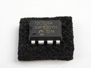
Der PIC12C509A wird häufig in eingebetteten Systemen verwendet, von der Unterhaltungselektronik bis hin zu Automobilanwendungen. Viele dieser Systeme sind jedoch mit Schutzmaßnahmen ausgestattet, um unbefugten Zugriff zu verhindern. Unser Service ermöglicht es Ihnen, diese Sicherheitsebenen zu durchbrechen und den zugrunde liegenden Quellcode aus den binären oder hexadezimalen Firmwaredateien abzurufen.
Ganz gleich, ob Ihr Ziel darin besteht, die Firmware zu klonen, zu duplizieren oder zu kopieren, unser Team verwendet fortschrittliche Reverse-Engineering-Techniken, um die gesicherten Binärdaten anzugreifen. Dieser Prozess umfasst häufig das Zerlegen der Firmware, das Analysieren der Programmlogik und das Extrahieren aussagekräftiger Daten, die für die weitere Verwendung neu entwickelt werden können. Wir können Ihnen helfen, die verborgenen Geheimnisse der Firmware zu entschlüsseln, um notwendige Anpassungen vorzunehmen, Fehler zu beheben, die Funktionalität zu verbessern oder Sicherheitsprüfungen durchzuführen.
Our Expertise in Handling Secured Data
Our reverse engineering service for the PIC12C509A binary involves using the latest tools and methods to open locked firmware, decrypt protected data, and extract the source code. By doing so, we provide a reliable solution to ensure you can make informed decisions about your embedded system, whether it’s for customization, repair, or vulnerability testing.
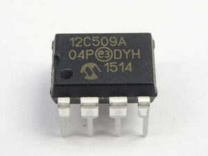
Нашата услуга за обратно инженерство за двоичния PIC12C509A включва използването на най-новите инструменти и методи за отваряне на заключен фърмуер, дешифриране на защитени данни и извличане на изходния код. Правейки това, ние предоставяме надеждно решение, за да гарантираме, че можете да вземате информирани решения относно вашата вградена система, независимо дали става въпрос за персонализиране, поправка или тестване на уязвимости.
Conclusion
If you’re struggling with locked or encrypted PIC12C509A firmware, our team is here to help. We can reverse engineer your microcontroller’s binary to restore functionality, break protective layers, and give you the tools to control and modify your embedded system. Contact us today to discuss your reverse engineering needs.
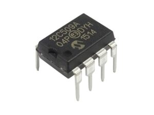
Nếu bạn đang gặp khó khăn với chương trình cơ sở PIC12C509A bị khóa hoặc mã hóa, nhóm của chúng tôi ở đây để giúp bạn. Chúng tôi có thể đảo ngược kỹ thuật nhị phân của bộ vi điều khiển của bạn để khôi phục chức năng, phá vỡ các lớp bảo vệ và cung cấp cho bạn các công cụ để kiểm soát và sửa đổi hệ thống nhúng của bạn. Liên hệ với chúng tôi ngay hôm nay để thảo luận về nhu cầu kỹ thuật đảo ngược của bạn.
PIC12C5XX memory is organized into program memory and data memory to facilitate the process of Reverse Engineering Microcontroller PIC12C509A Binary. For devices with more than 512 bytes of program memory, a paging scheme is used.
Program memory pages are accessed using one STATUS register bit. For the PIC12C509, PIC12C509A, PICCR509A and PIC12CE519 with a data memory register file of more than 32 registers, a banking scheme is used. Data memory banks are accessed using the File Select Register (FSR) for the purpose of Recover Chip PIC16F83 Eeprom.
The PIC12C5XX devices have a 12-bit Program Counter (PC) capable of addressing a 2K x 12 program memory space. Only the first 512 x 12 (0000h-01FFh) for the PIC12C509A and 1K x 12 (0000h-03FFh) for the PIC12C509, PIC12C509A, PIC12CR509A, and PIC12CE519 are physically implemented.
Refer to Figure 4-1. Accessing a location above these boundaries will cause a wrap around within the first 512 x 12 space (PIC12C509A) or 1K x 12 space (PIC12C509A) if Reverse engineering Microcontroller. The effective reset vector is at 000h, (see Figure 4-1). Location 01FFh (PIC12C508, PIC12C508A and PIC12CE518) or location 03FFh (PIC12C509, PIC12C509A, PIC12CR509A and PIC12CE519) contains the internal clock oscillator calibration value. This value should never be overwritten when Reverse Engineering Microcontroller PIC16C717 Program.
As a program instruction is executed, the Program Counter (PC) will contain the address of the next program instruction to be executed. The PC value is increased by one every instruction cycle, unless an instruction changes the PC.
For a GOTO instruction, bits 8:0 of the PC are provided by the GOTO instruction word. The PC Latch (PCL) is mapped to PC<7:0>. Bit 5 of the STATUS register provides page information to bit 9 of the PC (Figure 4- 8).For a CALL instruction, or any instruction where the PCL is the destination, bits 7:0 of the PC again are provided by the instruction word. However, PC<8> does not come from the instruction word, but is always cleared.
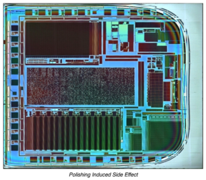
Reverse Engineering Microcontroller PIC12C509A Binary
Instructions where the PCL is the destination, or Modify PCL instructions, include MOVWF PC, ADDWF PC, and BSF PC,5. The Program Counter is set upon a RESET, which means that the PC addresses the last location in the last page i.e., the oscillator calibration instruction. After executing MOVLW XX, the PC will roll over to location 00h, and begin executing user code through Break IC PIC16C711 Program.
The STATUS register page preselect bits are cleared upon a RESET, which means that page 0 is pre-selected. Therefore, upon a RESET, a GOTO instruction will automatically cause the program to jump to page 0 until the value of the page bits is altered by Crack MCU.
 Reverse Engineering Microcontroller PIC16C558A Eeprom
Microcontrollers like the PIC16C558A store critical firmware and data in their internal EEPROM, often under protective security measures to prevent unauthorized access. However, in various scenarios—such as legacy system recovery, security analysis, or system optimization—it becomes necessary to restore, decrypt, or duplicate the locked firmware for further use. We specialize in Reverse Engineering Microcontroller PIC16C558A EEPROM, offering professional solutions to decode and clone its embedded program.
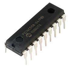
Az olyan mikrokontrollerek, mint a PIC16C558A, a kritikus firmware-t és adatokat belső EEPROM-jukban tárolják, gyakran biztonsági intézkedések mellett, hogy megakadályozzák az illetéktelen hozzáférést. Különféle forgatókönyvek esetén azonban – például a régi rendszer-helyreállításban, biztonsági elemzésben vagy rendszeroptimalizálásban – szükségessé válik a zárolt firmware visszaállítása, visszafejtése vagy másolása a további használathoz. Szakterületünk a PIC16C558A EEPROM Reverse Engineering mikrokontroller, amely professzionális megoldásokat kínál a beágyazott program dekódolására és klónozására.
Unlocking Protected PIC16C558A EEPROM
The PIC16C558A EEPROM is designed with secured features to prevent unauthorized access, but our advanced firmware decryption and binary analysis techniques allow us to attack these security barriers and retrieve the original heximal source code. Using specialized hardware and software tools, we can copy, extract, and restore the flash memory, providing a complete binary file for modification or further study.
PIC16C558A EEPROM разработан с защищенными функциями для предотвращения несанкционированного доступа, но наши передовые методы дешифрования прошивки и двоичного анализа позволяют нам атаковать эти барьеры безопасности и извлекать исходный шестнадцатеричный код. Используя специализированные аппаратные и программные инструменты, мы можем копировать, извлекать и восстанавливать флэш-память, предоставляя полный двоичный файл для модификации или дальнейшего изучения.
Our Expertise in Microcontroller Hacking and Cloning
- EEPROM Data Extraction – We use cutting-edge techniques to unlock and decrypt the secured firmware stored in flash memory.
- Reverse Engineering & Decompilation – Our team converts binary code into readable source code, making it easier to analyze and modify.
- Firmware Duplication & Cloning – Whether you need to duplicate, clone, or open an archived program, we ensure high accuracy and reliability.
- Security Research & Debugging – Identifying vulnerabilities in protected microcontrollers is crucial for debugging and cybersecurity assessments.
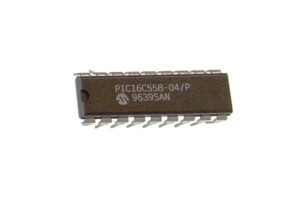
Nossa experiência em hacking e clonagem de microcontroladores
Extração de dados EEPROM – Usamos técnicas de ponta para desbloquear e descriptografar o firmware protegido armazenado na memória flash.
Engenharia reversa e descompilação – Nossa equipe converte código binário em código-fonte legível, facilitando a análise e a modificação.
Duplicação e clonagem de firmware – Se você precisa duplicar, clonar ou abrir um programa arquivado, garantimos alta precisão e confiabilidade.
Pesquisa e depuração de segurança – Identificar vulnerabilidades em microcontroladores protegidos é crucial para avaliações de depuração e segurança cibernética.
Why Choose Us?
- Proven expertise in microcontroller reverse engineering
- Advanced tools for breaking encrypted EEPROM firmware
- Confidential and secure services tailored to client needs
At [Your Company Name], we help you crack, copy, and decrypt PIC16C558A EEPROM firmware with precision. Contact us today to discuss your project and recover valuable memory files from locked microcontrollers!
The clock input (OSC1/CLKIN pin) is internally divided by four to generate four non-overlapping quadrature clocks namely Q1, Q2, Q3 and Q4. Internally, the program counter (PC) is incremented every Q1 if Reverse Engineering Microcontroller PIC16C558A Eeprom, the instruction is fetched from the program memory and latched into the instruction register in Q4. The instruction is decoded and executed during the following Q1 through Q4..
An “Instruction Cycle” consists of four Q cycles (Q1, Q2, Q3 and Q4). The instruction fetch and execute are pipelined such that fetch takes one instruction cycle while decode and execute takes another instruction cycle similar to the process of Reverse Engineering Microcontroller PIC16F73 Program.
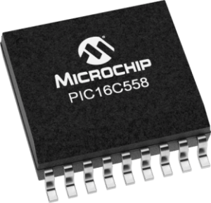
Reverse Engineering Microcontroller PIC16C558A Eeprom
However, due to the pipelining, each instruction effectively executes in one cycle. If an instruction causes the program counter to change (e.g., GOTO) then two cycles are required to complete the instruction (Example 3-1) after Reverse engineering Microcontroller. A fetch cycle begins with the program counter (PC) incrementing in Q1.
In the execution cycle, the fetched instruction is latched into the “Instruction Register (IR)” in cycle Q1. This instruction is then decoded and executed during the Q2, Q3, and Q4 cycles. Data memory is read during Q2 (operand read) and written during Q4 (destination write).
The PIC16C55X(A) has a 13-bit program counter capable of addressing an 8K x 14 program memory space. Only the first 512 x 14 (0000h – 01FFh) for the PIC16C554(A), 1K x 14 (0000h – 03FFh) for the PIC16C556A and 2K x 14 (0000h – 07FFh) for the PIC16C558(A) are physically implemented.
Accessing a location above these boundaries will cause a wrap-around within the first 512 x 14 space PIC16C554(A) or 1K x 14 space PIC16C556A or 2K x 14 space PIC16C558(A). The reset vector is at 0000h and the interrupt vector is at 0004h when Recover MCU PIC16F74A Binary.
The data memory (Figure 4-4 and Figure 4-5) is partitioned into two Banks which contain the general purpose registers and the special function registers. Bank 0 is selected when the RP0 bit is cleared. Bank 1 is selected when the RP0 bit (STATUS <5>) is set.
The Special Function Registers are located in the first 32 locations of each Bank. Register locations 20-6Fh (Bank0) on the PIC16C554(A)/556A and 20-7Fh (Bank0) and A0-BFh (Bank1) on the PIC16C558(A) are general purpose registers implemented as static RAM when Reverse Engineering Microcontroller PIC16C558A Eeprom. Some special purpose registers are mapped in Bank 1
 Reverse Engineering Microcontroller PIC16C554 Software
We can Reverse engineering Microcontroller PIC16C554 Software, please view the Microcontroller PIC16C554 features for your reference:
High Performance RISC CPU:
· Only 35 instructions to learn
· All single-cycle instructions (200 ns), except for program branches which are two-cycle
· Operating speed:
– DC – 20 MHz clock input
– DC – 200 ns instruction cycle
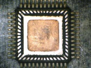
फ़र्मवेयर एक्सट्रैक्शन – विशेष हार्डवेयर और सॉफ़्टवेयर टूल का उपयोग करके, हम माइक्रोकंट्रोलर से लॉक किए गए फ़्लैश और EEPROM मेमोरी को कॉपी और डिक्रिप्ट करते हैं, जिससे इसमें संग्रहीत बाइनरी या हेक्सिमल प्रोग्राम की पूरी पुनर्प्राप्ति सुनिश्चित होती है।
बाइनरी विश्लेषण और डिसअसेम्बली – एक बार निकाले जाने के बाद, फ़र्मवेयर बाइनरी का सावधानीपूर्वक विश्लेषण किया जाता है, असेंबली भाषा में डिसअसेम्बल किया जाता है, और अधिक पठनीय प्रारूप में परिवर्तित किया जाता है। यह चरण हमें एन्क्रिप्टेड इंस्ट्रक्शन सेट को डिकोड करने और सोर्स कोड संरचना को फिर से बनाने में मदद करता है।
डिकंपाइलेशन और कोड पुनर्निर्माण – उन्नत डिकंपाइलेशन तकनीकों को लागू करके, हम संरक्षित प्रोग्राम को C-जैसे सोर्स कोड प्रारूप में पुनर्स्थापित करते हैं, जिससे नए हार्डवेयर प्लेटफ़ॉर्म के लिए एम्बेडेड सॉफ़्टवेयर को संशोधित, अनुकूलित या क्लोन करना आसान हो जाता है।
रीप्रोग्रामिंग और डुप्लीकेशन – रिवर्स इंजीनियरिंग के बाद, हम माइक्रोकंट्रोलर फ़र्मवेयर को डुप्लिकेट कर सकते हैं, जिससे क्लाइंट बैकअप कॉपी बना सकते हैं, सुरक्षित प्रोग्राम को क्लोन कर सकते हैं या इसे किसी अन्य संगत डिवाइस में स्थानांतरित कर सकते हैं।
16 special function hardware registers can help to IC program crack
Special Microcontroller Features (cont’d)
8-level deep hardware stack
Direct, Indirect and Relative addressing modes
Programmable code protection against Extract IC program
Power saving SLEEP mode
Peripheral Features:
· 13 I/O pins with individual direction control
· High current sink/source for direct LED drive Selectable oscillator options Serial in-circuit programming (via two pins) Four user programmable ID locations
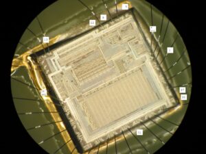
Firmware-Extraktion – Mithilfe spezieller Hard- und Softwaretools kopieren und entschlüsseln wir den gesperrten Flash- und EEPROM-Speicher des Mikrocontrollers und stellen so die vollständige Wiederherstellung des darin gespeicherten Binär- oder Hexadezimalprogramms sicher.
Binäranalyse und -disassemblierung – Nach der Extraktion wird die Firmware-Binärdatei sorgfältig analysiert, in Assemblersprache disassembliert und in ein besser lesbares Format konvertiert. Dieser Schritt hilft uns, den verschlüsselten Befehlssatz zu entschlüsseln und die Quellcodestruktur zu rekonstruieren.
Dekompilierung und Code-Rekonstruktion – Durch den Einsatz fortschrittlicher Dekompilierungstechniken stellen wir das geschützte Programm in ein C-ähnliches Quellcodeformat wieder her. Dies erleichtert die Änderung, Optimierung oder das Klonen der eingebetteten Software für neue Hardwareplattformen.
Neuprogrammierung und -duplizierung – Nach dem Reverse Engineering können wir die Mikrocontroller-Firmware duplizieren, sodass Kunden Sicherungskopien erstellen, das gesicherte Programm klonen oder auf ein anderes kompatibles Gerät übertragen können.
· Timer0: 8-bit timer/counter with 8-bit programmable prescaler
Special Microcontroller Features:
· Power-on Reset (POR)
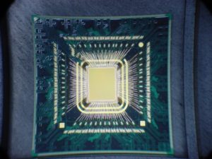
Reverse Engineering Microcontroller PIC16C554 Software
· Power-up Timer (PWRT) and Oscillator Start-up Timer (OST)
· Watchdog Timer (WDT) with its own on-chip RC oscillator for reliable operation
CMOS Technology:
· Low-power, high-speed CMOS EPROM technology
· Fully static design
· Wide operating voltage range
– 2.5V to 5.5V PIC16C55X
– 3.0 to 5.5V PIC16C55XA
· Commercial, industrial and extended temperature range
· Low power consumption
– < 2.0 mA @ 5.0V, 4.0 MHz
– 15 µA typical @ 3.0V, 32 kHz
– < 1.0 µA typical standby current @ 3.0V
Circuit Engineering Company Limited continues to be recognized as the Southern China Leader in Services for IC Read, MCU Crack, Chip Reverse engineering, Microcontroller Unlock service. With the advancement of today’s modern circuit board technology, it is more important than ever to have specialists available to help you at a moment’s notice. Our engineering and commercial teams collectively have a vast amount of electronic experience covering field include Consumer Electronics, Industrial Automation Electronics, Wireless Communication Electronics., etc. For more information please contact us through email.
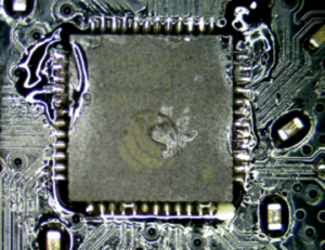
펌웨어 추출 – 특수 하드웨어 및 소프트웨어 도구를 사용하여 마이크로컨트롤러에서 잠긴 플래시 및 EEPROM 메모리를 복사하고 해독하여 내부에 저장된 바이너리 또는 16진수 프로그램을 완전히 검색합니다.
바이너리 분석 및 분해 – 추출된 펌웨어 바이너리는 신중하게 분석되고 어셈블리 언어로 분해되어 더 읽기 쉬운 형식으로 변환됩니다. 이 단계는 암호화된 명령어 세트를 디코딩하고 소스 코드 구조를 재구성하는 데 도움이 됩니다.
디컴파일 및 코드 재구성 – 고급 디컴파일 기술을 적용하여 보호된 프로그램을 C와 유사한 소스 코드 형식으로 복원하여 새로운 하드웨어 플랫폼에 대한 임베디드 소프트웨어를 수정, 최적화 또는 복제하는 것을 더 쉽게 만듭니다.
재프로그래밍 및 복제 – 리버스 엔지니어링 후 마이크로컨트롤러 펌웨어를 복제하여 클라이언트가 백업 사본을 만들거나 보안된 프로그램을 복제하거나 다른 호환 장치로 전송할 수 있습니다.
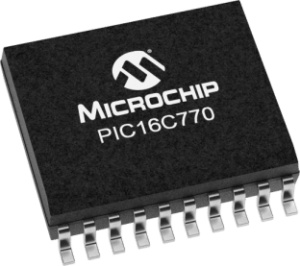
 Read Chip PIC16C770 Eeprom
This document contains device-specific information and necessary info for Read Chip PIC16C770 Eeprom. Additional information may be found in the PICmicroTM Mid-Range Reference Manual, (DS33023), which may be obtained from your local Microchip Sales Representative or downloaded from the Microchip website.
The Reference Manual should be considered a complementary document to this data sheet, and is highly recommended reading for a better understanding of the device architecture and operation of the peripheral modules.
There are two memory blocks in each of these PICmicro ® microcontrollers. Each block (Program Memory and Data Memory) has its own bus, so that concurrent access can occur. Additional information on device memory may be found in the PICmicro Mid-Range Reference Manual, (DS33023).
The PIC16C770 devices have a 13-bit program counter capable of addressing an 8K x 14 program memory space. The PIC16C717 and the PIC16C770 have 2K x 14 words of program memory by Break IC PIC16F685 Code. The PIC16C771 has 4K x 14 words of program memory. Accessing a location above the physically implemented address will cause a wraparound.
The reset vector is at 0000h and the interrupt vector is at 0004h. Each bank extends up to 7Fh (128 bytes). The lower locations of each bank are reserved for the Special Function Registers. Above the Special Function Registers are General Purpose Registers, implemented as static RAM when Unlock Microcontroller.
All implemented banks contain special function registers. Some frequently used special function registers from one bank are mirrored in another bank for code reduction and quicker access in order to Attack IC PIC12F510 Program. The Special Function Registers are registers used by the CPU and Peripheral Modules for controlling the desired operation of the device. These registers are implemented as static RAM.
The special function registers can be classified into two sets; core (CPU) and peripheral. Those registers associated with the core functions are described in detail in this section. Those related to the operation of the peripheral features are described in detail in that peripheral feature section.
 Reverse Engineering Microcontroller PIC16C717 Program
We can Reverse engineering Microcontroller PIC16C717 Program, please view the Microcontroller PIC16C717 features for your reference:
Microcontroller Core Features:
· High-performance RISC CPU
· Only 35 single word instructions to learn
· All single cycle instructions except for program branches which are two cycle
· Operating speed: DC – 20 MHz clock input
· Interrupt capability (up to 10 internal/external interrupt sources)
· Eight level deep hardware stack to prove the difficulty of Read CPLD Chip Microcontroller IC JED
· Direct, indirect and relative addressing modes
· Power-on Reset (POR)
· Power-up Timer (PWRT) and Oscillator Start-up Timer (OST)
· Watchdog Timer (WDT) with its own on-chip RC oscillator for reliable operation when Extract PLD Chip Eeprom
· Selectable oscillator options:
– INTRC – Internal RC, dual speed (4MHz and 37KHz) dynamically switchable for power savings
– ER – External resistor, dual speed (user selectable frequency and 37KHz) dynamically switchable for power savings
– EC – External clock
– HS – High speed crystal/resonator
– XT – Crystal/resonator
– LP – Low power crystal
· Low-power, high-speed CMOS EPROM technology which can help to ease the process of Copy CPLD MCU software data
· In-Circuit Serial Programming™ (ISCP)
· Wide operating voltage range: 2.5V to 5.5V
· 15 I/O pins with individual control for:
– Direction (15 pins)
– Digital/Analog input (6 pins)
– PORTB interrupt on change (8 pins)
– PORTB weak pull-up (8 pins)
– High voltage open drain (1 pin)
· Commercial and Industrial temperature ranges
· Low-power consumption:
– < 2 mA @ 5V, 4 MHz
– 22.5 µA typical @ 3V, 32 kHz
· Timer0: 8-bit timer/counter with 8-bit prescaler
· Timer1: 16-bit timer/counter with prescaler, can be incremented during sleep via external crystal/clock
· Timer2: 8-bit timer/counter with 8-bit period register, prescaler and postscaler
· Enhanced Capture, Compare, PWM (ECCP) module
– Capture is 16 bit, max. resolution is 12.5 ns
– Compare is 16 bit, max. resolution is 200 ns
– PWM max. resolution is 10 bit
– Enhanced PWM:
– Single, Half-Bridge and Full-Bridge output modes
– Digitally programmable deadband delay
· Analog-to-Digital converter:
– PIC16C770/771 12-bit resolution
– PIC16C717 10-bit resolution
· On-chip absolute bandgap voltage reference generator
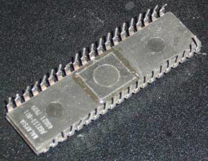
Reverse Engineering Microcontroller PIC16C717 Program
· Programmable Brown-out Reset (PBOR) circuitry
· Programmable Low-Voltage Detection (PLVD) circuitry
· Master Synchronous Serial Port (MSSP) with two modes of operation:
– 3-wire SPI™ (supports all 4 SPI modes)
– I2C™ compatible including master mode support only
· Program Memory (PMR) capability for look-up table, character string storage and checksum calculation purposes
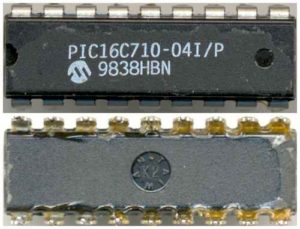
 Reverse Engineering Microcontroller PIC16C710 Code
We can Reverse Engineering Microcontroller PIC16C710 Code, please view the Microcontroller PIC16C710 features for your reference:
· High-performance RISC CPU
· Only 35 single word instructions to learn
· All single cycle instructions except for program branches which are two cycle
· Operating speed: DC – 20 MHz clock input DC – 200 ns instruction cycle
· Up to 2K x 14 words of Program Memory, up to 128 x 8 bytes of Data Memory (RAM)
· Interrupt capability
· Eight level deep hardware stack
· Direct, indirect, and relative addressing modes
· Power-on Reset (POR)
· Power-up Timer (PWRT) and Oscillator Start-up Timer (OST)
· Watchdog Timer (WDT) with its own on-chip RC oscillator for reliable operation only after Attack MCU PIC16C558 Program
· Programmable code-protection
· Power saving SLEEP mode
· Selectable oscillator options
· Low-power, high-speed CMOS EPROM technology
· Fully static design
· Wide operating voltage range: 2.5V to 6.0V
· High Sink/Source Current 25/25 mA
· Commercial, Industrial and Extended temperature ranges
· Program Memory Parity Error Checking Circuitry with Parity Error Reset (PER) (PIC16C715)
· Low-power consumption:
– < 2 mA @ 5V, 4 MHz
– 15 µA typical @ 3V, 32 kHz
– < 1 µA typical standby current
Circuit Engineering Company Limited continues to be recognized as the Southern China Leader in Services for IC Read, MCU Crack, Chip Reverse engineering, Microcontroller reverse engineering service.
With the advancement of today’s modern circuit board technology, it is more important than ever to have specialists available to help you at a moment’s notice after Reverse Engineering Microcontroller PIC16C710 Code.
Our engineering and commercial teams collectively have a vast amount of electronic experience covering field include Consumer Electronics, Industrial Automation Electronics, Wireless Communication Electronics., etc. For more information please contact us through email.
 Reverse Engineering Microcontroller PIC16C76 Heximal
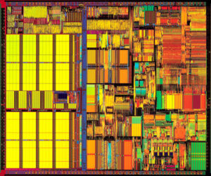
Reverse Engineering Microcontroller PIC16C76 Heximal
Any instruction which writes, operates internally as a read followed by a write operation. The BCF and BSF instructions, for example, read the register into the CPU, execute the bit operation and write the result back to the register. Caution must be used when these instructions are applied to a port with both inputs and outputs defined after Reverse engineeringMicrocontroller.
For example, a BSF operation on bit5 of PORTB will cause all eight bits of PORTB to be read into the CPU. Then the BSF operation takes place on bit5 and PORTB is written to the output latches.
If another bit of PORTB is used as a bi-directional I/O pin (e.g., bit0) and it is defined as an input at this time, the input signal present on the pin itself would be read into the CPU and rewritten to the data latch of this particular pin, overwriting the previous content.
As long as the pin stays in the input mode, no problem occurs. However, if bit0 is switched to an output, the content of the data latch may now be unknown.
Reading the port register, reads the values of the port pins. Writing to the port register writes the value to the port latch. When using read-modify-write instructions (ex.BCF, BSF, etc.) on a port, the value of the port pins is read, the desired operation is done to this value, and this value is then written to the port latch.
Example 5-4 shows the effect of two sequential read-modify-write instructions on an I/O port. A pin actively outputting a Low or High should not be driven from external devices at the same time in order to change the level on this pin (“wired-or”, “wired-and”). The resulting high output currents may damage the chip when Crack MCU.
The actual write to an I/O port happens at the end of an instruction cycle, whereas for reading, the data must be valid at the beginning of the instruction cycle. Therefore, care must be exercised if a write followed by a read operation is carried out on the same I/ O port.
The sequence of instructions should be such to allow the pin voltage to stabilize (load dependent) before the next instruction which causes that file to be read into the CPU is executed.
Otherwise, the previous state of that pin may be read into the CPU rather than the new state. When in doubt, it is better to separate these instructions with a NOP or another instruction not accessing this I/O port.
It can directly interface to an 8-bit microprocessor data bus. The external microprocessor can read or write the PORTD latch as an 8-bi t latch when Copy MCU PIC12C509 Program. Setting bit PSPMODE enables port pin RE0/RD/AN5 to be the RD input, RE1/WR/AN6 to be the WR input and RE2/CS/AN7 to be the CS (chip select) input.
For this functionality, the corresponding data direction bits of the TRISE register (TRISE<2:0>) must be configured as inputs (set) and the A/D port configuration bits PCFG2:PCFG0 (ADCON1<2:0>) must be set, which will configure pins RE2:RE0 as digital I/O after Reverse Engineering Microcontroller PIC16C76 Heximal.
 Copy Chip PIC16C73A Program
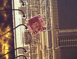
Copy Chip PIC16C73A Program
The Synchronous Serial Port can be configured as either a 3-wire Serial Peripheral Interface (SPI) or the two-wire Inter-Integrated Circuit (I2C) bus which can help to facilitate the process of Copy Chip PIC16C73A Program. The Universal Synchronous Asynchronous Receiver Transmitter (USART) is also known as the Serial Communications Interface or SCI. Also a 5-channel high-speed 8-bit A/D is provided.
The 8-bit resolution is ideally suited for applications requiring low-cost analog interface, e.g. thermostat control, pressure sensing, etc.
The PIC16C74/74A devices have 192 bytes of RAM, while the PIC16C77 has 368 bytes of RAM. Each device has 33 I/O pins. In addition several peripheral features are available including: three timer/counters, two Capture/Compare/PWM modules and two serial ports.
The Synchronous Serial Port can be configured as either a 3-wire Serial Peripheral Interface (SPI) or the two-wire Inter-Integrated Circuit (I2C) bus. The Universal Synchronous Asynchronous Receiver Transmitter (USART) is also known as the Serial Communications Interface or SCI which can be used to Break Microcontroller PIC16F628A Content.
An 8-bit Parallel Slave Port is provided. Also an 8-channel high-speed 8-bit A/D is provided after Copy Chip. The 8-bit resolution is ideally suited for applications requiring low-cost analog interface, e.g. thermostat control, pressure sensing, etc.
The PIC16C7X family has special features to reduce external components, thus reducing cost, enhancing system reliability and reducing power consumption.
There are four oscillator options, of which the single pin RC oscillator provides a low-cost solution, the LP oscillator minimizes power consumption, XT is a standard crystal, and the HS is for High Speed crystals.
The SLEEP (power-down) feature provides a power saving mode. The user can wake up the chip from SLEEP through several external and internal interrupts and resets to faciliate the process of Break MCU PIC16F631 Flash. A highly reliable Watchdog Timer with its own on-chip RC oscillator provides protection against software lock-up.
A UV erasable CERDIP packaged version is ideal for code development while the cost-effective One-Time-Programmable (OTP) version is suitable for production in any volume.
The PIC16C7X family fits perfectly in applications ranging from security and remote sensors to appliance control and automotive. The EPROM technology makes customization of application programs (transmitter codes, motor speeds, receiver frequencies, etc.) extremely fast and convenient.
The small footprint packages make this microcontroller series perfect for all applications with space limitations when Copy Chip. Low cost, low power, high performance, ease of use and I/O flexibility make the PIC16C7X very versatile even in areas where no microcontroller use has been considered before Attack Microcontroller PIC16C710 Program (e.g. timer functions, serial communication, capture and compare, PWM functions and coprocessor applications).
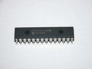
 Reverse Engineering Microcontroller PIC16F73 Program
We can Reverse engineering Microcontroller PIC16F73 Program, please view the Microcontroller PIC16F73 features for your reference:
The PIC16C7X is a family of low-cost, high-performance, CMOS, fully-static, 8-bit microcontrollers with integrated analog-to-digital (A/D) converters, in the PIC16CXX mid-range family.
All PIC16/17 microcontrollers employ an advanced RISC architecture. The PIC16CXX microcontroller family has enhanced core features, eight-level deep stack, and multiple internal and external interrupt sources.
The separate instruction and data buses of the Harvard architecture allow a 14-bit wide instruction word with the separate 8-bit wide data. The two stage instruction pipeline allows all instructions to execute in a single cycle, except for program branches which require two cycles.
A total of 35 instructions (reduced instruction set) are available. Additionally, a large register set gives some of the architectural innovations used to achieve a very high performance. PIC16CXX microcontrollers typically achieve a 2:1 code compression and a 4:1 speed improvement over other 8-bit microcontrollers in their class.
The PIC16C72 has 128 bytes of RAM and 22 I/O pins. In addition several peripheral features are available including: three timer/counters, one Capture/Compare/PWM module and one serial port. The Synchronous Serial Port can be configured as either a 3-wire Serial Peripheral Interface (SPI) or the two-wire Inter-Integrated Circuit (I 2C) bus.
Also a 5-channel high-speed 8-bit A/D is provided. The 8-bit resolution is ideally suited for applications requiring low-cost analog interface, e.g. thermostat control, pressure sensing, etc.
The PIC16C73 devices have 192 bytes of RAM, while the PIC16C76 has 368 byes of RAM. Each device has 22 I/O pins. In addition, several peripheral features are available including: three timer/counters, two Capsuited for applications requiring low-cost analog interface, e.g. thermostat control, pressure sensing, etc only when Attack IC PIC12F510 Program.
The PIC16C7X family has special features to reduce external components, thus reducing cost, enhancing system reliability and reducing power consumption.
There are four oscillator options, of which the single pin RC oscillator provides a low-cost solution, the LP oscillator minimizes power consumption, XT is a standard crystal, and the HS is for High Speed crystals.
The SLEEP (power-down) feature provides a power saving mode. The user can wake up the chip from SLEEP through several external and internal interrupts and resets in order to Copy IC PIC12C509A Binary.
A highly reliable Watchdog Timer with its own on-chip RC oscillator provides protection against software lock up. A UV erasable CERDIP packaged version is ideal for code development while the cost-effective One-Time-Programmable (OTP) version is suitable for production in any volume.
The PIC16C7X family fits perfectly in applications ranging from security and remote sensors to appliance control and automotive. The EPROM technology makes customization of application programs (transmitter codes, motor speeds, receiver frequencies, etc.) extremely fast and convenient when Reverse Engineering Microcontroller PIC16F73 Program.
The small footprint packages make this microcontroller series perfect for all applications with space limitations. Low cost, low power, high performance, ease of use and I/O flexibility make the PIC16C7X very versatile even in areas where no microcontroller use has been considered (e.g. timer functions, serial communication, capture and compare, PWM functions and coprocessor applications).
 Reverse Engineering Microcontroller PIC16C622 Program
PIC16C62X devices have special features to reduce external components, thus reducing system cost, enhancing system reliability and reducing power consumption to Reverse Engineering Microcontroller PIC16C622 Program. There are four oscillator options, of which the single pin RC oscillator provides a low-cost solution, the LP oscillator minimizes power consumption, XT is a standard crystal, and the HS is for High Speed crystals.
The SLEEP (power-down) mode offers power savings. The user can wake up the chip from SLEEP through several external and internal interrupts and reset.
A highly reliable Watchdog Timer with its own on-chip RC oscillator provides protection against software lock- up.
A UV-erasable CERDIP-packaged version is ideal for code development while the cost-effective One-Time Programmable (OTP) version is suitable for production in any volume.
Table 1-1 shows the features of the PIC16C62X mid-range microcontroller families.
A simplified block diagram of the PIC16C62X is shown in below Figure.
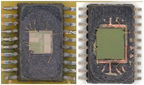
Reverse Engineering Microcontroller PIC16C622 Program
The PIC16C62X series fit perfectly in applications ranging from battery chargers to low-power remote sensors. The EPROM technology makes customization of application programs (detection levels, pulse generation, timers, etc.) extremely fast and convenient. The small footprint packages make this microcontroller series perfect for all applications with space limitations. Low-cost, low-power, high-performance, ease of use and I/O flexibility make the PIC16C62X very versatile from Reverse Engineering Microcontroller PIC16C622 Program.
Circuit Engineering Company Limited continues to be recognized as the Southern China Leader in Services for IC Read, MCU Reverse engineering, Chip Extract, Microcontroller Unlock service. With the advancement of today’s modern circuit board technology, it is more important than ever to have specialists available to help you at a moment’s notice. Our engineering and commercial teams collectively have a vast amount of electronic experience covering field include Consumer Electronics, Industrial Automation Electronics, Wireless Communication Electronics., etc. For more information please contact us through email.
