Archive for the ‘Reverse Engineer Microcontroller’ Category
 Reverse TMS320F28022 Microcontroller Locked Flash Memory
reverse engineering TMS320F28022PTT secured microcontroller locked flash memory after unlock MCU TMS320F28022PTT protection system and readout the embedded firmware of binary file or eeprom memory heximal data from original microprocessor TMS320F28022PTT;
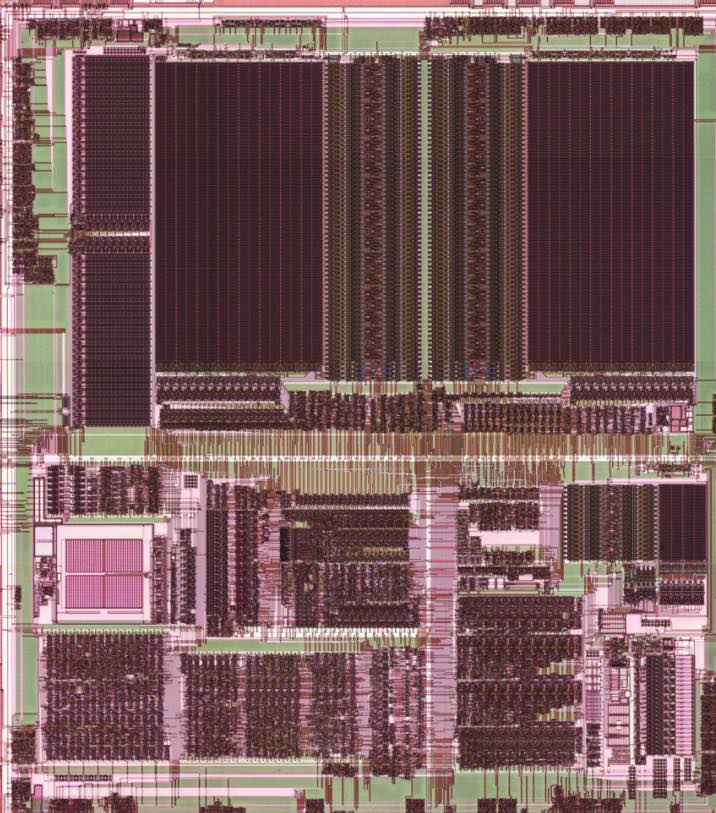
As with many DSP type devices, multiple busses are used to move data between the memories and peripherals and the CPU. The C28x memory bus architecture contains a program read bus, data read bus and data write bus. The program read bus consists of 22 address lines and 32 data lines.
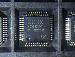
ingeniería inversa TMS320F28022PTT microcontrolador asegurado memoria flash bloqueada después de desbloquear el sistema de protección MCU TMS320F28022PTT y leer el firmware integrado del archivo binario o datos heximales de la memoria eeprom del microprocesador original TMS320F28022PTT;
The data read and write busses consist of 32 address lines and 32 data lines each. The 32-bit-wide data busses enable single cycle 32-bit operations. The multiple bus architecture, commonly termed Harvard Bus, enables the C28x to fetch an instruction, read a data value and write a data value in a single cycle.
All peripherals and memories attached to the memory bus will prioritize memory accesses to reverse tms320f28016 flash code. Generally, the priority of memory bus accesses can be summarized as follows:
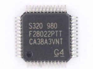
зваротная распрацоўка TMS320F28022PTT, абароненая флэш-памяць, заблакіраваная мікракантролерам, пасля разблакіроўкі MCU, сістэма абароны TMS320F28022PTT і счытванне ўбудаванай прашыўкі двайковага файла або памяці eeprom, шаснаццаткавыя дадзеныя з арыгінальнага мікрапрацэсара TMS320F28022PTT;
Highest:
Data Writes (Simultaneous data and program writes cannot occur on the memory bus.)
Program Writes (Simultaneous data and program writes cannot occur on the memory bus.)
Data Reads Program
(Simultaneous program reads and fetches cannot occur on the Reads memory bus.)
Lowest:
Fetches (Simultaneous program reads and fetches cannot occur on the memory bus.)
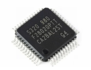
tersine mühendislik TMS320F28022PTT, MCU TMS320F28022PTT koruma sisteminin kilidini açtıktan ve orijinal mikroişlemci TMS320F28022PTT’den ikili dosya veya eeprom belleğinin onaltılık verilerinin yerleşik donanım yazılımını okuduktan sonra güvenli mikro denetleyici kilitli flash bellek;
 Reverse Engineering TMS320F28016 Microprocessor Flash Code
Reverse Engineering TMS320F28016 Microprocessor Flash Firmware is a process to unlock tms320f28016 dsp mcu security fuse bit, then extract embedded source code from microcontroller;
Interface to memory and I/O devices of varying speeds is accomplished by using the READY input. When transactions are made with slower devices, the TMS320F28016 processor waits until the other device completes its function and signals the processor by way of the READY input.
Once a ready indication is provided from the external device, execution continues. On the ’x240 device, the READY input must be driven (active high) to complete reads or writes to internal data I/O-memory-mapped registers and all external addresses only.
The bus request (BR) signal is used in conjunction with the other TMS320F28016 interface signals to arbitrate external global-memory accesses. Global memory is external data-memory space in which the BR signal is asserted at the beginning of the access.
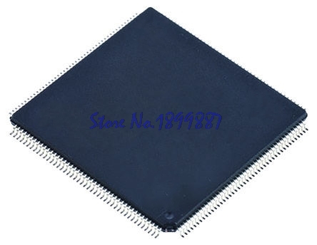
When an external global-memory device receives the bus request, it responds by asserting the ready signal after the global-memory access is arbitrated and the global access is completed.
The TMS320F28016 supports zero-wait-state reads on the external interface. However, to avoid bus conflicts, writes take two cycles. This allows the ’x240 to buffer the transition of the data bus from input to output (or output to input) by a half cycle by breaking mcu tms320f28021 mcu memory. In most systems, TMS320F28016 ratio of reads to writes is significantly large to minimize the overhead of the extra cycle on writes.
Wait states can be generated when accessing slower external resources. The wait states operate on machine-cycle boundaries and are initiated either by using the ready signal or using the software wait-state generator to recover microcontroller tms320f28012pgfa firmware. Ready can be used to generate any number of wait states.
 Break Microchip PIC18F44K22 Controller Flash Memory
Break Microchip PIC18F44K22 Controller Flash Memory and crack mcu pic18f44k22 protective system then readout embedded firmware fro microcontroller;
The external Resistor-Capacitor (RC) modes support the use of an external RC circuit. This allows the designer maximum flexibility in frequency choice while keeping costs to a minimum when clock accuracy is not required. There are two modes: RC and RCIO.
In RC mode, the RC circuit connects to OSC1. OSC2/ CLKOUT outputs the RC oscillator frequency divided by 4. This signal may be used to provide a clock for external circuitry in order to faciliate the process of breaking microchip mcu pic18f14k22 flash memory, synchronization, calibration, test or other application requirements. Figure 2-8 shows the external RC mode connections.
In RCIO mode, the RC circuit is connected to OSC1. OSC2 becomes a general purpose I/O pin.
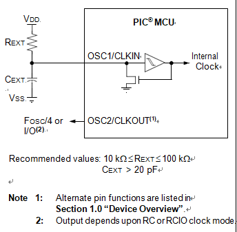
The RC oscillator frequency is a function of the supply voltage, the resistor (REXT) and capacitor (CEXT) values and the operating temperature. Other factors affecting the oscillator frequency are:
- input threshold voltage variation
- component tolerances
- packaging variations in capacitance
The user also needs to take into account variation due to tolerance of external RC components used.
 PLD Chip Reverse Engineering
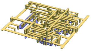
In the case that property holder and defendant are competitors in the semiconductor industry. The property holder produced a PLD (Programmable Logic Device) chip to perform various logic functions. defendant produces different types of chips, called ASIC (Application-Specific Integrated Circuit), which performs different functions than the property holder’s chip. However, the property holder believes that the layout design of the chip ASIC produced by the defendant (called the mask work in the United States) duplicated layout design that he registered which is obtained from PLD Chip Reverse Engineering.
PLD Chip Reverse Engineering clause on the one hand protects the interests of the owner of the layout design and on the other hand promotes technological innovation. In PLD reverse engineering, the second layout design must not be substantially the same as the first layout design.
As long as there is evidence that substantial investment and effort has been made in the development of the update new layout design, not just 100% cloning, it does not constitute infringement, even if the two layout designs are similar in some substantive parts.
The law actually allows competitors to copy microcontroller layout designs, but only if the purpose of reproduction is to develop their own original layout design.
As long as a PLD layout design embodies a low degree of creativity in any aspect, it can be considered original, and the requirements for creativity here are quite low.
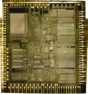
In the Microcontroller reverse engineering process, competitors can take pictures and copy the registered layout design, but if competitors use this information to produce a substantially identical layout design, then it cannot be called legal reverse engineering. 1 Legal reverse engineering refers to taking pictures and copying layout designs, but the purpose of photographing and copying is to analyze the research, and combine the results of analysis and research into their own layout design to generate unique and genuine Layout design.
 Reverse Engineering Microcontroller Layout Design
Infringer further argued that Reverse Engineering Microcontroller Layout Design on the core unit of the copyright holder layout design. It proposes that, according to the law, if the microcontroller layout design is developed through reverse engineering, then it is not necessary to bear the tort liability.
In the instructions given to the jury, the court pointed out that if the non-rights person reverse engineered and studied the layout design of others’ microcontroller, analyzed the circuit structure, and then integrated the analysis results into his own layout design, it did not constitute infringement.
The instructions emphasize that if infringer’s layout design contains its own new design elements, an improvement or an alternative to the copyright holder layout design, then the layout design is original.
It also explains that the layout design obtained through reverse engineering can be considered as original and therefore does not constitute infringement, but only if it is not substantially similar to the protected layout design, and its design contains significant Hard work and commitment, not just copying.
The instructions also remind the jury to focus on whether the defendant’s layout design is an original microcontroller layout design obtained through reverse engineering.
Infringer pointed out that it has made a lot of investment in the process of developing microcontroller layout design, and the Semiconductor Chip Protection Act prohibits the investment of very small plagiarism, rather than the reverse engineering behavior that has invested a lot of time and energy.
It also presented a paper trail to prove that it was a mcu reverse engineering rather than a simple microcontroller copy. Infringer has always stressed that he has no intention of copying copyright holder’s layout design, and he has not done so. As can be seen from the written traces, Infringer spent more than $3 million and two and a half years to analyze copyright holder’s layout design.
Infringer points out that if you want to copy copyright holder’s layout design, it only takes a few months, not a few years. At the same time, Infringer proposed that its controlled semiconductor chip is smaller and faster than copyright holder’s chip.
 Microcontroller Reverse Engineering Behavior
In the development of the Integrated circuit industry, Microcontroller Reverse Engineering behavior is common. This behavior is beneficial to designing integrated circuit products with the same basic functions but better performance, smaller size and lower cost.
The technological advancement of the integrated circuit industry does not unduly violate the principle of fair competition. Therefore, countries generally recognize the legitimacy of microcontroller reverse engineering behavior in the Integrated circuit protection law, which makes reverse engineering IC an important defense tools for integrated circuit copyright infringement.
However, reverse engineering is method to dissipate and acquire the key technology of other designer (property owner). On the basis of this, the layout design obtained will inevitably contain the imitation and microcontroller copying of the prior layout design, so it is easy to be confused with the infringement, thus causing disputes.
Therefore, it is very necessary to make an accurate distinction between infringement and reverse engineering behavior. On the one hand, it helps to protect the legal rights of the owner of the layout design, avoids the infringer’s use of reverse engineering IC as a defense tool to escape legal sanctions, and on the other hand enables the person implementing reverse engineering to correctly assess the legal risk of his behavior. To understand whether it is possible to suspect infringement litigation and how to circumvent it, so that the integrated circuit industry will develop in a healthy and orderly direction.
On the basis of introducing the basic knowledge of integrated circuit, circuitry layout design and MCU reverse engineering, the article focuses on the judgment standard of integrated circuit infringement and the judgment standard of microcontroller reverse engineering behavior, thus clarifying the relationship between infringement and reverse engineering behavior.
 Decapsulate Microcontroller Silicon Package
Decapsulate Microcontroller Silicon Package which has helped to provide the protection over the chip wafer from moisture and air, microcontroller can be decapsulated using 100% Nitric acid heated to 60°C. It was added in small drops and washed away with acetone after a few seconds.
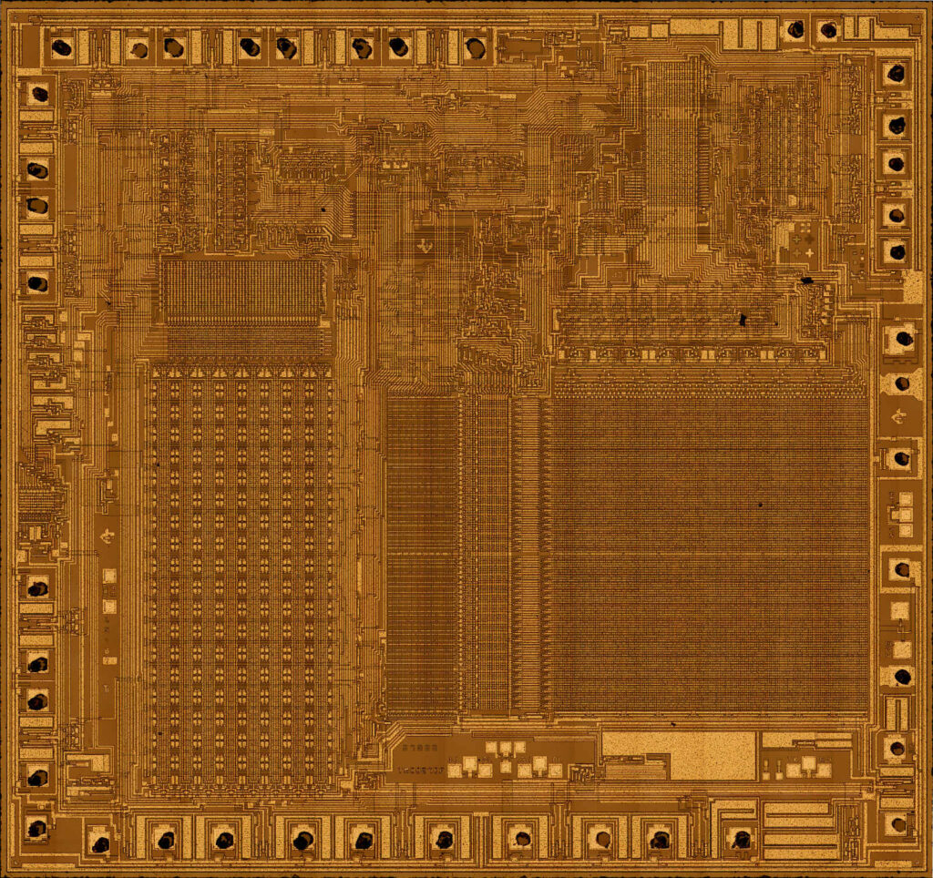
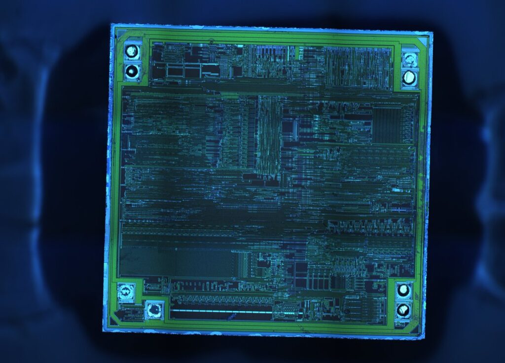
This MCU decapsulation process was repeated for several minutes until the surface of the chip die was exposed. Although the bonding wires were also exposed, this did not create any short circuits because of the high concentration of the acid. Once the IC decapsulation was finished, the whole sample was cleaned in acetone using ultrasonic bath. That removed the remaining of the acid and particles of resin. As a result the surface of the chip became clean. After careful removal of the tapes and testing the device demonstrated full functionality (below Figure).
It is very important to make sure that the microcontroller is not over-decapsulated. This would result in the acid going into contact with PCB traces made of copper. They react very actively with acid and this will quickly result in loss contact with bonding wires. The device with live battery connection could then be used for further IC extraction of the embedded SRAM using microprobing MCU attacks.
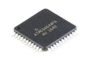
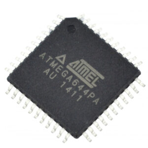
 Reverse Engineering Microcontroller ATmega644PA Firmware
Reverse engineering Microcontroller ATmega644PA firmware involves decoding and analyzing the embedded firmware stored within its flash memory program. Engineers often seek to recover or clone this microcontroller’s source code for testing, replication, or troubleshooting purposes. The ATmega644PA, known for its robust design in embedded systems, stores critical program instructions as binary data in EEPROM and flash memory, ensuring reliable functionality.
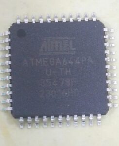
Beim Reverse Engineering der Firmware des Mikrocontrollers ATmega644PA geht es um das Dekodieren und Analysieren der eingebetteten Firmware, die in seinem Flash-Speicherprogramm gespeichert ist. Ingenieure versuchen häufig, den Quellcode dieses Mikrocontrollers zu Test-, Replikations- oder Fehlerbehebungszwecken wiederherzustellen oder zu klonen. Der ATmega644PA, der für sein robustes Design in eingebetteten Systemen bekannt ist, speichert kritische Programmbefehle als Binärdaten im EEPROM und Flash-Speicher und gewährleistet so eine zuverlässige Funktionalität.
To break through security features protecting this firmware, reverse engineering techniques must be employed to decode the program into a readable heximal file. This file format allows engineers to analyze the binary data and reconstruct the original source code, providing insights into how the microcontroller operates under different conditions. Recovering and cloning the ATmega644PA’s firmware requires precision to avoid data corruption, particularly as accessing EEPROM memory data often triggers security locks.
By managing each stage of the reverse engineering process carefully, engineers can maintain the integrity of the microcontroller’s program, ensuring any recovered source code is accurate and reliable. This process can be essential for device maintenance, compatibility testing, or creating compatible hardware designs that rely on the ATmega644PA’s core functions.
Note that if a level triggered interrupt is used for wake-up from Power-down mode, the changed level must be held for some time to wake up the procedures of Reverse Engineering Microcontroller ATmega644PA Firmware.
Refer to “External Interrupts”. When waking up from Power-down mode, there is a delay from the wake-up condition occurs until the wake-up becomes effective by Recover IC ST62T65C6 Software. This allows the clock to restart and become stable after having been stopped.
रिवर्स इंजीनियरिंग माइक्रोकंट्रोलर ATmega644PA फर्मवेयर में इसके फ्लैश मेमोरी प्रोग्राम में संग्रहीत एम्बेडेड फर्मवेयर को डिकोड करना और उसका विश्लेषण करना शामिल है। इंजीनियर अक्सर परीक्षण, प्रतिकृति या समस्या निवारण उद्देश्यों के लिए इस माइक्रोकंट्रोलर के स्रोत कोड को पुनर्प्राप्त या क्लोन करना चाहते हैं। एम्बेडेड सिस्टम में अपने मजबूत डिजाइन के लिए जाना जाने वाला ATmega644PA, महत्वपूर्ण प्रोग्राम निर्देशों को EEPROM और फ्लैश मेमोरी में बाइनरी डेटा के रूप में संग्रहीत करता है, जिससे विश्वसनीय कार्यक्षमता सुनिश्चित होती है।
The wake-up period is defined by the same CKSEL Fuses that define the Reset Time-out period, as described in “Clock Sources” on page 40. When the SM2..0 bits are written to 011, the SLEEP instruction makes the MCU Cracking enter Power-save mode.
This mode is identical to Power-down, with one exception: If Timer/Counter2 is enabled, it will keep running during sleep. The device can wake up from either Timer Overflow or Output Compare event from Timer/Counter2 if the corresponding Timer/Counter2 interrupt enable bits are set in TIMSK2 to facilitate the process of Attack MCU MSP430G2452IPW14R Heximal, and the Global Interrupt Enable bit in SREG is set.
If Timer/Counter2 is not running, Power-down mode is recommended instead of Power-save mode. The Timer/Counter2 can be clocked both synchronously and asynchronously in Power-save mode. If the Timer/Counter2 is not using the asynchronous clock, the Timer/Counter Oscillator is stopped during sleep.
سیستم عامل میکروکنترلر ATmega644PA مهندسی معکوس شامل رمزگشایی و تجزیه و تحلیل سیستم عامل تعبیه شده ذخیره شده در برنامه حافظه فلش خود است. مهندسان اغلب به دنبال بازیابی یا شبیه سازی کد منبع این میکروکنترلر برای اهداف آزمایش، تکرار یا عیب یابی هستند. ATmega644PA که به دلیل طراحی قوی خود در سیستمهای تعبیهشده شناخته میشود، دستورالعملهای برنامه حیاتی را به عنوان دادههای باینری در EEPROM و حافظه فلش ذخیره میکند و از عملکرد قابل اعتماد اطمینان میدهد.
If the Timer/Counter2 is not using the synchronous clock, the clock source is stopped during sleep. Note that even if the synchronous clock is running in Power-save, this clock is only available for the Timer/Counter2 in order to Attack IC TMS320F28232PGFA Software.
When the SM2..0 bits are 110 and an external crystal/resonator clock option is selected, the SLEEP instruction makes the MCU enter Standby mode. This mode is identical to Power-down with the exception that the Oscillator is kept running. From Standby mode, the device wakes up in six clock cycles.
 Break MCU ATmega128PA Firmware
The Atmel® AVR® core combines a rich instruction set with 32 general purpose working registers. All the 32 registers are directly connected to the Arithmetic Logic Unit (ALU) which can provide great support for Break MCU ATmega128PA Firmware, allowing two independent registers to be accessed in one single instruction executed in one clock cycle.
The resulting architecture is more code efficient while achieving throughputs up to ten times faster than conventional CISC microcontrollers in order to Copy IC PIC16F886 Firmware. The ATmega128 provides the following features: 128Kbytes of In-System Programmable Flash with Break-While-Write capabilities, 4Kbytes EEPROM, 4Kbytes SRAM, 53 general purpose I/O lines, 32 general purpose working registers, Real Time Counter (RTC), four flexible Timer/Counters with compare modes and PWM, 2 USARTs, a byte oriented Two-wire Serial Interface, an 8-channel, 10-bit ADC with optional differential input stage with programmable gain, programmable Watchdog Timer with Internal Oscillator, an SPI serial port, IEEE std. 1149.1 compliant JTAG test interface, also used for accessing the On-MCU Debug system and programming and six software selectable power saving modes if Break MCU ATMEGA128PA Firmware.
The Idle mode stops the CPU while allowing the SRAM, Timer/Counters, SPI port, and interrupt system to continue functioning. The Power-down mode saves the register contents but freezes the Oscillator, disabling all other MCU functions until the next interrupt or Hardware Reset before Copy MCU AT89C55WD Binary. In Power-save mode, the asynchronous timer continues to run, allowing the user to maintain a timer base while the rest of the device is sleeping for the purpose of Break MCU ATmega128PA Firmware. The ADC Noise Reduction mode stops the CPU and all I/O modules except Asynchronous Timer and ADC, to minimize switching noise during ADC conversions. In Standby mode, the Crystal/Resonator Oscillator is running while the rest of the device is sleeping.
This allows very fast start-up combined with low power consumption. In Extended Standby mode, both the main Oscillator and the Asynchronous Timer continue to run. Atmel offers the QTouch® library for embedding capacitive touch buttons, sliders and wheels functionality into AVR microcontrollers. The patented charge-transfer signal acquisition offers robust sensing and includes fully debounced reporting of touch keys and includes Adjacent Key Suppression® (AKS™) technology for unambiguous detection of key events. The easy-to-use QTouch Suite toolchain allows you to explore, develop and debug your own touch applications when Break MCU ATMEGA128PA Firmware.
The device is manufactured using Atmel’s high-density nonvolatile memory technology. The On-MCU ISP Flash allows the program memory to be reprogrammed in-system through an SPI serial interface, by a conventional nonvolatile memory programmer, or by an On-MCU Boot program running on the AVR core to provide great support for Break MCU ATmega128PA Firmware. The boot program can use any interface to download the application program in the application Flash memory.
Software in the Boot Flash section will continue to run while the Application Flash section is updated, providing true Break-While-Write operation. By combining an 8-bit RISC CPU with In-System Self-Programmable Flash on a monolithic MCU, the Atmel ATmega128 is a powerful microcontroller that provides a highly flexible and cost effective solution to many embedded control applications after Attack Microcontroller W77E058A40DL Flash. The ATmega128 device is supported with a full suite of program and system development tools including: C compilers, macro assemblers, program debugger/simulators, in-circuit emulators, and evaluation kits.
 Break MCU AT87LV51 Software
We can Break MCU AT87LV51 Software, please view the Mcu AT87LV51 features for your reference:
The AT87LV51 is a low-voltage, high-performance CMOS 8-bit mcu with 4K bytes of QuickFlash One-Time Programmable (OTP) memory when Recover MCU Microchip CF755 Dump. The device is manufactured using Atmel’s high-density nonvolatile memory technology and is compatible with the industry standard MCS-51 instruction set and pinout.
The on-chip QuickFlash allows the program memory to be user programmed by a conventional nonvolatile memory programmer. By combining a versatile 8-bit CPU with QuickFlash on a monolithic chip, the Atmel AT87LV51 is a powerful mcu that provides a highly flexible and cost-effective solution to many embedded control applications.
The AT87LV51 provides the following standard features: 4K bytes of QuickFlash OTP program memory, 128 bytes of RAM, 32 I/O lines, two 16-bit timer/counters, a five-vector, 2-level interrupt architecture, a full duplex serial port, on-chip oscillator, and clock circuitry. In addition, the AT87LV51 is designed with static logic for operation down to zero frequency and supports two software-selectable power-saving modes after Break MCU AT87LV51 Software.
The Idle mode stops the CPU while allowing the RAM, timer/counters, serial port and interrupt system to continue functioning. The Power-down mode saves the RAM contents but freezes the oscillator disabling all other chip functions until the next hardware reset. XTAL1 and XTAL2 are the input and output, respectively, of an inverting amplifier, which can be configured for use as an on-chip oscillator.
Either a quartz crystal or ceramic resonator may be used. To drive the device from an external clock source, XTAL2 should be left unconnected while XTAL1 is driven as shown in below Figure. There are no requirements on the duty cycle of the external clock signal, since the input to the internal clocking circuitry is through a divide-by-two flip-flop, but minimum and maximum voltage high and low time specifications must be observed.
In Idle Mode, the CPU puts itself to sleep while all the on chip peripherals remain active. The mode is invoked by software. The content of the on-chip RAM and all the Special Function registers remains unchanged during this mode. The Idle mode can be terminated by any enabled interrupt or by a hardware reset when Break MCU AT87LV51 Software.
It should be noted that when Idle is terminated by a hardware reset, the device normally resumes program execution from where it left off, up to two machine cycles before the internal reset algorithm takes control. On-chip hardware inhibits access to internal RAM in this event to Unlock Microcontroller, but access to the port pins is not inhibited.
To eliminate the possibility of an unexpected write to a port pin when Idle is terminated by reset, the instruction following the one that invokes Idle should not be one that writes to a port pin or to external memory.
