Archive for the ‘Reverse Engineer Microcontroller’ Category
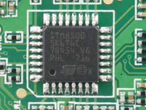
 STMicro STM8S207S8 microprocessor reverse engineering
STMicro STM8S207S8 microprocessor reverse engineering can help engineer to break mcu stm8s207s8 protection and restore microcontroller stm8s207s8 memory program from flash and data from eeprom;
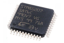
STMicro STM8S207S8 microprocessor reverse engineering can help engineer to break mcu stm8s207s8 protection and restore microcontroller stm8s207s8 memory program from flash and data from eeprom;
The read-out protection blocks reading and writing the Flash program memory and data EEPROM memory in ICP mode (and debug mode). Once the read-out protection is activated, any attempt to toggle its status triggers a global erase of the program and data memory.
Even if no protection can be considered as totally unbreakable, the feature provides a very high level of protection for a general purpose microcontroller when recover stm8s003k3 flash memory heximal file.
The clock controller distributes the system clock (fMASTER) coming from different oscillators to the core and the peripherals. It also manages clock gating for low power modes and ensures clock robustness.
Clock prescaler: To get the best compromise between speed and current consumption the clock frequency to the CPU and peripherals can be adjusted by a programmable prescaler.
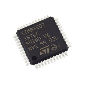
STMicro STM8S207S8 mikroişlemci tersine mühendisliği, mühendisin MCU STM8S207S8 korumasını kırmasına ve mikrodenetleyici STM8S207S8 bellek programını flaştan ve EEPROM’dan gelen verilerden geri yüklemesine yardımcı olabilir
Safe clock switching: Clock sources can be changed safely on the fly in run mode through a configuration register. The clock signal is not switched until the new clock source is ready. The design guarantees glitch-free switching.
Clock management: To reduce power consumption, the clock controller can stop the clock to the core, individual peripherals or memory.
Master clock sources: Four different clock sources can be used to drive the master clock:
1-24 MHz high-speed external crystal (HSE)
Up to 24 MHz high-speed user-external clock (HSE user-ext)
16 MHz high-speed internal RC oscillator (HSI)
128 kHz low-speed internal RC (LSI)
Startup clock: After reset, the microcontroller restarts by default with an internal 2 MHz clock (HSI/8). The prescaler ratio and clock source can be changed by the application program as soon as the code execution starts from cloning stm8s103f2 mcu memory source code.
Clock security system (CSS): This feature can be enabled by software. If an HSE clock failure occurs, the internal RC (16 MHz/8) is automatically selected by the CSS and an interrupt can optionally be generated.
Configurable main clock output (CCO): This outputs an external clock for use by the application.
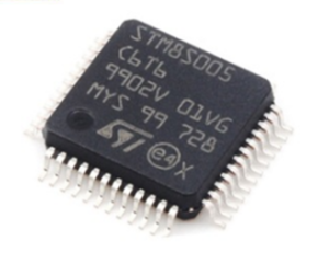
 Reverse MCU STM8S005C6T6 Flash Memory Code
Reverse MCU STM8S005C6T6 Flash Memory Code and readout embedded firmware from microprocessor stm8s005c6 memory, crack microcontroller stm8s005c6 fuse bit and remove its protective over the flash memory;
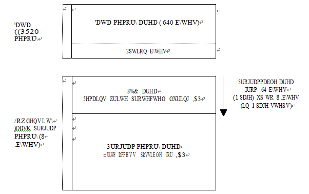
This divides the program memory into two areas:
Main program memory: up to 8 Kbyte minus UBC
User-specific boot code (UBC): Configurable up to 8 Kbyte
inversez le code de la mémoire flash MCU STM8S005C6T6 et lisez le micrologiciel intégré à partir de la mémoire du microprocesseur stm8s005c6, craquez le bit de fusible du microcontrôleur stm8s005c6 et retirez sa protection sur la mémoire flash ;
The UBC area remains write-protected during in-application programming. This means that the MASS keys do not unlock the UBC area when break stm8s103f3 micro cpu flash memory. It protects the memory used to store the boot program, specific code libraries, reset and interrupt vectors, the reset routine and usually the IAP and communication routines.
The read-out protection blocks reading and writing the Flash program memory and data EEPROM memory in ICP mode (and debug mode) which can be disable by breaking stm8s105 protective memory fuse bit.
Once the read-out protection is activated, any attempt to toggle its status triggers a global erase of the program and data memory. Even if no protection can be considered as totally unbreakable, the feature provides a very high level of protection for a general purpose microcontroller.
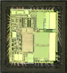
 Reverse Engineering Microcontroller STM8S105K6U3 Structure
Reverse Engineering Microcontroller STM8S105K6U3 Structure can help us to figure out the security fuse bit of MCU stm8s105k6 location, then we can crack mcu stm8s105k6 memory protective system and readout embedded firmware from MCU;
Single wire interface module (SWIM) and debug module (DM)
The single wire interface module and debug module permits non-intrusive, real-time in- circuit debugging and fast memory programming.
SWIM
Single wire interface module for direct access to the debug module and memory programming. The interface can be activated in all device operation modes to copy stm8s003f3 mcu flash memory content, The maximum data transmission speed is 145 bytes/ms.
Debug module
The non-intrusive debugging module features a performance close to a full-featured emulator. Beside memory and peripherals, also CPU operation can be monitored in real- time by means of shadow registers.
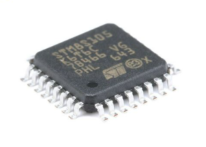
La structure du microcontrôleur d’ingénierie inverse STM8S105K6U3 peut nous aider à comprendre le bit de fusible de sécurité de l’emplacement du MCU stm8s105k6, puis nous pouvons craquer le système de protection de la mémoire mcu stm8s105k6 et lire le micrologiciel intégré du MCU
R/W to RAM and peripheral registers in real-time
R/W access to all resources by stalling the CPU
Breakpoints on all program-memory instructions (software breakpoints)
Two advanced breakpoints, 23 predefined configurations
Interrupt controller
Nested interrupts with three software priority levels,
32 interrupt vectors with hardware priority in the process of breaking microprocessor stm8s105k4 flash memory,
Up to 27 external interrupts on 6 vectors including TLI,
Trap and reset interrupts
Flash program and data EEPROM memory
8 Kbyte of Flash program single voltage Flash memory,
640 byte true data EEPROM,
User option byte area.
 Microchip IC PIC18F26K83 Flash Heximal File Cloning
Microchip IC PIC18F26K83 Flash Heximal File Cloning needs to unlock MICROCHIP PIC18F26K83 protection over its flash and eeprom memory, then replicate secured memory program of mcu pic18f26k83;
256 Bytes Data EEPROM
Programmable Code Protection
Direct, Indirect and Relative Addressing modes
Up to 32K bytes Program Flash Memory
Up to 2048 Bytes Data SRAM Memory
Operating Voltage Ranges:
– 1.8V to 3.6V (PIC18LF24/25K40 )
– 2.3V to 5.5V ( PIC18F24/25K40)
Temperature Range:
Industrial: -40°C to 85°C
Extended: -40°C to 125°C
Doze: CPU and Peripherals Running at Different Cycle Rates (typically CPU is lower)
Idle: CPU Halted While Peripherals Operate when breaking microchip mcu pic18f24k40 controller flash memory;
Sleep: Lowest Power Consumption
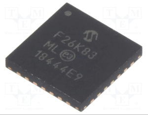
microchip IC PIC18F26K83 microcontrolador flash clonagem de arquivo heximal precisa desbloquear MICROCHIP PIC18F26K83 proteção sobre sua memória flash e eeprom, em seguida, replicar o programa de memória segura do MCU pic18f26k83;
Peripheral Module Disable (PMD):
Ability to selectively disable hardware module to minimize active power consumption of unused peripherals after reverse engineering mcu pic18f25k20 locked file;
Extreme Low-Power mode (XLP)
Sleep: 500 nA typical @ 1.8V
Sleep and Watchdog Timer: 900 nA typical @ 1.8V
Sleep mode: 50 nA @ 1.8V, typical
Windowed Watchdog Timer: 500 nA @ 1.8V, typical
Secondary Oscillator: 500 nA @ 32 kHz
Operating Current:
8 uA @ 32 kHz, 1.8V, typical
32 uA/MHz @ 1.8V, typical
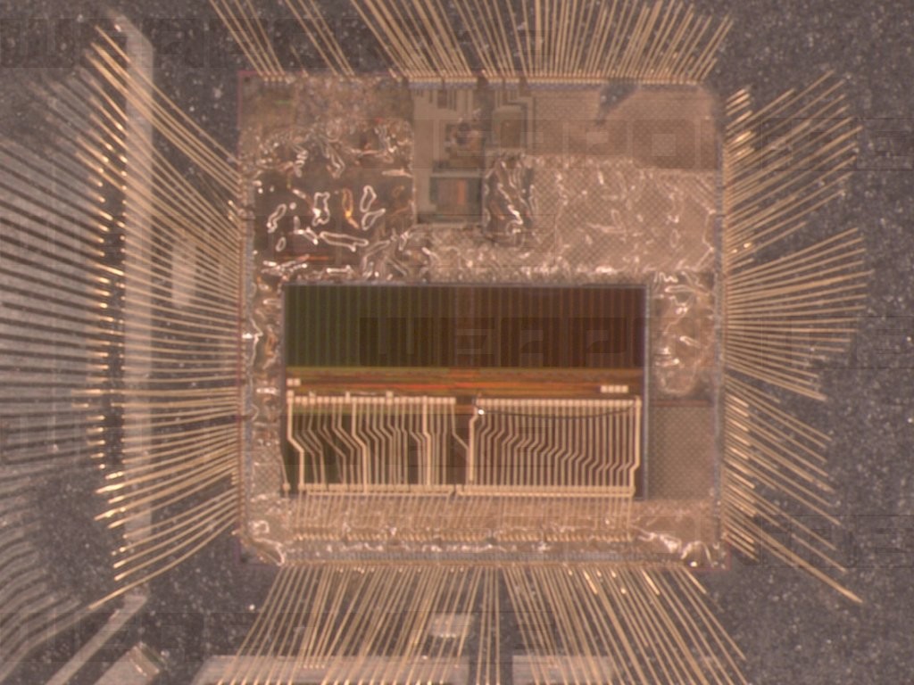
 Altera CPLD EPM7256ATC144 Chip Eeprom Data Decoding
Altera CPLD EPM7256ATC144 Chip Eeprom Data Decoding needs to crack altera pld epm7256atc protective system and reset the status of CPLD IC from locked to unlock, extract embedded software from IC CPLD chip;
- See the Operating Requirements for Altera Devices Data Sheet.
- Minimum DC input voltage is –0.5 V. During transitions, the inputs may undershoot to –2.0 V for input currents less than 100 mA and periods shorter than 20 ns.
- For EPM7128A and EPM7256A devices only, VCC must rise monotonically.
- In MAX 7000AE devices, all pins, including dedicated inputs, I/O pins, and JTAG pins, may be driven before VCCINT and VCCIO are powered.
- These devices support in-system programming for –40° to 100° C. For in-system programming support between –40° and 0° C, contact Altera Applications.
These values are specified under the recommended operating conditions shown in Table 14 on page 28.
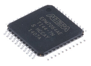
Le décodage de données de la puce Altera CPLD EPM7256ATC144 doit déchiffrer le système de protection Altera PLD EPM7256ATC et réinitialiser l’état de CPLD IC de verrouillé à déverrouiller, extraire le logiciel embarqué de la puce IC CPLD;
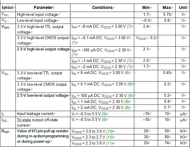
The parameter is measured with 50% of the outputs each sourcing the specified current. The IOH parameter refers to high-level TTL or CMOS output current for the purpose of recovering altera cpld epm7128alc eeprom program.
The parameter is measured with 50% of the outputs each sinking the specified current. The IOL parameter refers to low-level TTL or CMOS output current.
This value is specified for normal device operation. For MAX 7000AE devices, the maximum leakage current during power-up is ±300 mA. For EPM7128A and EPM7256A devices, leakage current during power-up is not specified which is especially useful features for recover cpld epm7032vtc system memory content.
(10) For EPM7128A and EPM7256A devices, this pull-up exists while a device is programmed in-system.
For MAX 7000AE devices, this pull-up exists while devices are programmed in-system and in unprogrammed devices during power-up.
Capacitance is measured at 25 °C and is sample-tested only. The OE1 pin (high-voltage pin during programming) has a maximum capacitance of 20 pF.
The POR time for MAX 7000AE devices (except MAX 7128A and MAX 7256A devices) does not exceed 100 ms. The sufficient VCCINT voltage level for POR is 3.0 V. The device is fully initialized within the POR time after VCCINT reaches the sufficient POR voltage level.
 Renesas Microcontroller M30835FJGP Flash Memory Binary Cloning
Renesas Microcontroller M30835FJGP Flash Memory Binary Cloning is a process to discover embedded firmware from mcu M30835FJGP and readout source code from processor;
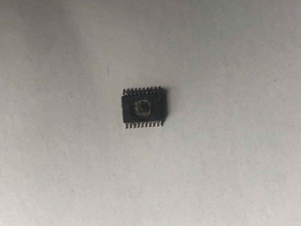
The M32C/83 Group (M32C/83, M32C/83T) microcomputer is a single-chip control unit that utilizes high performance silicon gate CMOS technology with the M32C/80 Series CPU core.
The M32C/83 Group (M32C/83, M32C/83T) is available in 144-pin and 100-pin plastic molded LQFP/QFP packages. With a 16-Mbyte address space, this microcomputer combines advanced instruction manipulation capabilities to process complex instructions by less bytes and execute instructions at higher speed when copying renesas m306nkfh microcontroller flash memory program.
La clonazione binaria del microcontrollore M30835FJGP della memoria flash Renesas è un processo per scoprire il firmware incorporato dall’MCU M30835FJGP e leggere il codice sorgente dal processore;
It includes a multiplier and DMAC adequate for office automation, communication devices and industrial equipments, and other high-speed processing applications.
| Characteristic | Performance | ||
| M32C/83 | M32C/83T | ||
| Basic Instructions | 108 instructions | ||
| Minimum Instruction Execution Time | 31.3 ns (f(BCLK) = 32 MHz, VCC = 4.2 to 5.5 V)50 ns (f(BCLK) = 20 MHz, VCC = 3.0 to 5.5 V) | 31.3 ns (f(BCLK) = 32 MHz, VCC=4.2 to 5.5 V) | |
| Operating Mode | Single-chip mode, Memory expansionmode and Microprocessor mode | Single-chip mode | |
| Address Space | 16 Mbytes | ||
| Memory Capacity | See Table 1.3 | ||
| I/O Port | 87 I/O pins and 1 input pin | ||
| Multifunction Timer | Timer A: 16 bits x 5 channels, Timer B: 16 bits x 6 channelsThree-phase motor control circuit | ||
| Intelligent I/O | Time measurement function: 16 bits x 5 channelsWaveform generating function: 16 bits x 10 channelsCommunication function (Clock synchronous serial I/O, Clock asynchronous se-rial I/O, HDLC data processing, Clock synchronous variable length serial I/O,(1)IEBus ) | ||
| Serial I/O | 5 Channels(1) 2 (2)Clock synchronous serial I/O, Clock asynchronous serial I/O, IEBus , I C bus | ||
| CAN Module | 1 channel Supporting CAN 2.0B specification | ||
| A/D Converter | 10-bit A/D converter: 2 circuits, 26 channels | ||
| D/A Converter | 8 bits x 2 channels | ||
| DMAC | 4 channels | ||
| DMAC II | Can be activated by all peripheral function interrupt sourcesImmediate transfer, Calculation transfer and Chain transfer functions | ||
| CRC Calculation Circuit | CRC-CCITT | ||
| X/Y Converter | 16 bits x 16 bits | ||
| Watchdog Timer | 15 bits x 1 channel (with prescaler) | ||
| Interrupt | 42 internal and 8 external sources, 5 software sourcesInterrupt priority level: 7 |
 Copy Renesas Microcontroller M306NKFHGP#U3 Flash Program
Copy Renesas Microcontroller M306NKFHGP#U3 Flash Program needs to disable the protection over MCU M306NKFHGP#U3 by hacking technology and then extract IC chip code from embedded flash memory;
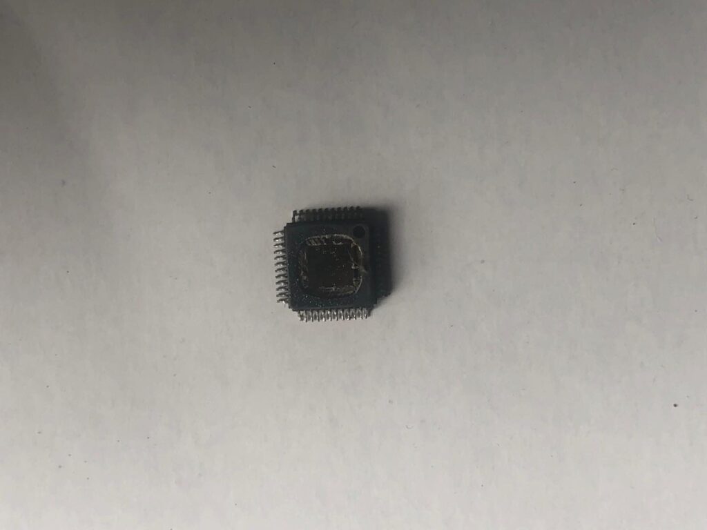
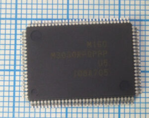
The M16C/6N Group (M16C/6N4) of MCUs are built using the high-performance silicon gate CMOS process using the M16C/60 Series CPU core and are packaged in 100-pin plastic molded QFP and LQFP.
These MCUs operate using sophisticated instructions featuring a high level of instruction efficiency. With 1 Mbyte of address space, they are capable of executing instructions at high speed when attacking renesas microcontroller r5f51115adfm3 flash memory. Being equipped with two CAN (Controller Area Network) modules in the M16C/6N Group (M16C/6N4), the MCU is suited to drive automotive and industrial control systems.
रेनेसास माइक्रोकंट्रोलर M306NKFHGP # यू 3 फ्लैश प्रोग्राम को हैकिंग तकनीक द्वारा एमसीयू M306NKFHGP # यू 3 पर सुरक्षा को अक्षम करने और फिर एम्बेडेड फ्लैश मेमोरी से आईसी चिप कोड निकालने की आवश्यकता है।
The CAN modules comply with the 2.0B specification. In addition, this MCU contains a multiplier and DMAC which combined with fast instruction processing capability, makes it suitable for control of various OA, communication, and industrial equipment which requires high-speed arithmetic/ logic operations.
1.1 Applications
· Automotive, industrial control systems and other automobile, other (T/V-ver. product)
· Car audio and industrial control systems, other (Normal-ver. product)
 Mixed Signal CPU MSP430G2231 Secured Flash Program Replicating
Mixed Signal CPU MSP430G2231 Secured Flash Program Replicating will refer to extract locked code in the format of heximal from texas instrument microprocessor msp430g2231 after unlock microcontroller msp430g2231 flash memory;
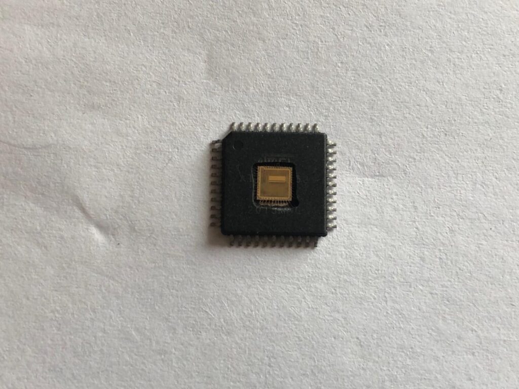
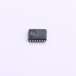
The clock system is supported by the basic clock module that includes support for a 32768-Hz watch crystal oscillator, an internal very-low-power low-frequency oscillator, an internal digitally-controlled oscillator (DCO), and a high-frequency crystal oscillator.
The basic clock module is designed to meet the requirements of both low system cost and low power consumption to reverse microcontroller msp430g2112 flash memory. The internal DCO provides a fast turn- on clock source and stabilizes in less than 1 µs. The basic clock module provides the following clock signals:
मिश्रित सिग्नल सीपीयू MSP430G2231 सुरक्षित फ्लैश प्रोग्राम प्रतिकृति माइक्रोकंट्रोलर एमएसपी 430 जी 2231 फ्लैश मेमोरी को अनलॉक करने के बाद टेक्सास इंस्ट्रूमेंट माइक्रोप्रोसेसर एमएसपी 430 जी 2231 से समीपस्थ के प्रारूप में लॉक कोड निकालने का उल्लेख करेगा;
Auxiliary clock (ACLK), sourced from a 32768-Hz watch crystal, a high-frequency crystal, or the internal very-low-power LF oscillator.
Main clock (MCLK), the system clock used by the CPU.
Sub-Main clock (SMCLK), the sub-system clock used by the peripheral modules. The brownout circuit is implemented to provide the proper internal reset signal to the device during power on and power off which can be used for restoring msp430g2001 microcontroller heximal program.
There are four 8-bit I/O ports implemented—ports P1, P2, P3, and P4:
All individual I/O bits are independently programmable.
Any combination of input, output, and interrupt condition is possible.
Edge-selectable interrupt input capability for all eight bits of port P1 and P2.
Read and write access to port-control registers is supported by all instructions. Each I/O has an individually programmable pullup or pulldown resistor.
 Texas Instrument MSP430G2152 Flash Memory Data Replicating
Texas Instrument MSP430G2152 Flash Memory Data Replicating starts from crack msp430g2152 microcontroller tamper resistance system and extract locked source code from embedded flash memory of msp430g2152 mcu;
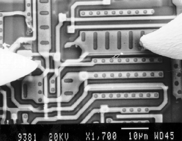
The primary function of the Comparator_A+module is to support precision slope analog-to-digital conversions, battery-voltage supervision, and monitoring of external analog signals.
The ADC10 module supports fast, 10-bit analog-to-digital conversions. The module implements a 10-bit SAR core, sample select control, reference generator and data transfer controller, or DTC, for automatic conversion result handling, allowing ADC samples to be converted and stored without any CPU intervention.
Die Replikation der Flash-Speicherdaten von Texas Instrument MSP430G2152 beginnt mit dem Crack-Manipulationsschutzsystem MSP430G2152 des Mikrocontrollers und extrahiert den gesperrten Quellcode aus dem eingebetteten Flash-Speicher der MCU msp430g2152
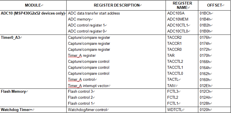
Stresses beyond those listed under “absolute maximum ratings” may cause permanent damage to the device. These are stress ratings only, and functional operation of the device at these or any other conditions beyond those indicated under “recommended operating conditions” is not implied when restore ti msp430g2101 flash content file. Exposure to absolute-maximum-rated conditions for extended periods may affect device reliability.
All voltages referenced to VSS. The JTAG fuse-blow voltage, VFB, is allowed to exceed the absolute maximum rating. The voltage is applied to the TEST pin when blowing the JTAG fuse and reverse reading msp430g2212 program file.
La replica dei dati della memoria flash Texas Instrument MSP430G2152 inizia dal sistema di resistenza alla manomissione del microcontrollore MSP430G2152 ed estrae il codice sorgente bloccato dalla memoria flash incorporata dell’MCU MSP430G2152
Higher temperature may be applied during board soldering according to the current JEDEC J-STD-020 specification with peak reflow temperatures not higher than classified on the device label on the shipping boxes or reels.
 Reverse Engineering DSP MCU TMS320F28034 Flash Memory
Reverse Engineering DSP MCU TMS320F28034 Flash Memory is a process to unlock microprocessor tms320f28034 flash protection and then readout the embedded binary from its processor memory;
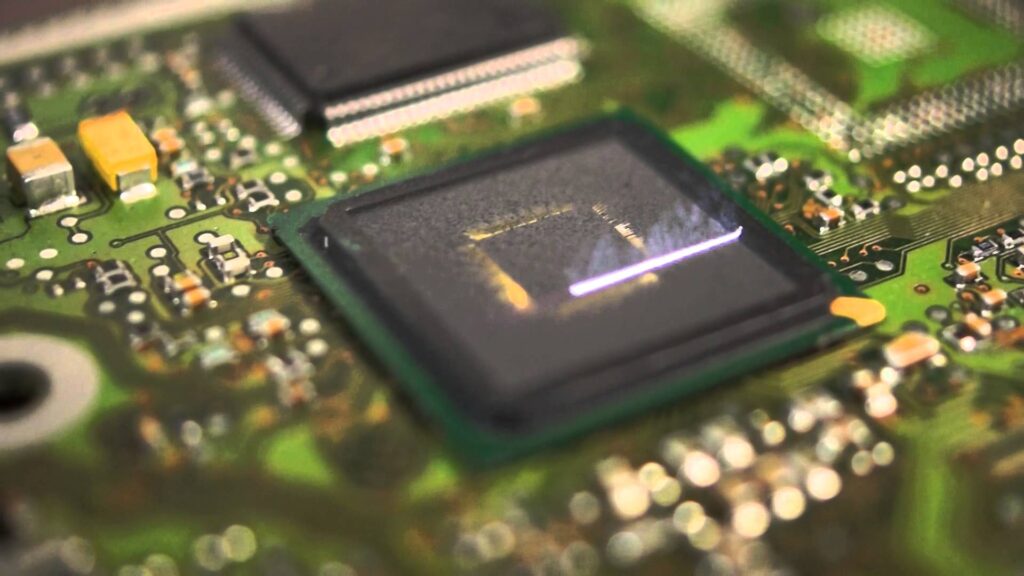
The 280x devices are full static CMOS devices. Three low-power modes are provided:
IDLE:
Place CPU into low-power mode. Peripheral clocks may be turned off selectively and only those peripherals that need to function during IDLE are left operating. An enabled interrupt from an active peripheral or the watchdog timer will wake the processor from IDLE mode in order to carry out the task of reverse engineering tms320f28016 microprocessor flash code.
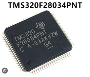
reverzní inženýrství DSP locked MCU TMS320F28034 systém odolnosti proti neoprávněné manipulaci a čtení firmware vestavěné flash paměti je proces prolomení šifrované flash ochrany mikroprocesoru TMS320F28034 a následné extrahování binárního kódu čipu MCU nebo heximálních dat z paměti jeho procesoru;
STANDBY:
Turns off clock to CPU and peripherals. This mode leaves the oscillator and PLL functional. An external interrupt event will wake the processor and the peripherals. Execution begins on the next valid cycle after detection of the interrupt event
HALT:
Turns off the internal oscillator. This mode basically shuts down the device and places it in the lowest possible power consumption mode. A reset or external signal can wake the device from this mode.
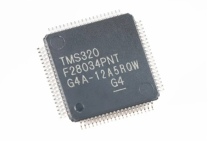
inginerie inversă DSP blocat MCU TMS320F28034 sistem de rezistență la manipulare și citire firmware-ul memoriei flash încorporate este un proces pentru a sparge protecția flash criptată a microprocesorului TMS320F28034 și apoi extrage codul binar sau datele heximale ale cipului MCU din memoria procesorului său;
The 280x segregate peripherals into three sections. The mapping of peripherals is as follows:
| PF0: | PIE: Flash: | PIE Interrupt Enable and Control Registers Plus PIE Vector Table Flash Control, Programming, Erase, Verify Registers |
| Timers: | CPU-Timers 0, 1, 2 Registers | |
| CSM: | Code Security Module KEY Registers | |
| ADC: | ADC Result Registers (dual-mapped) | |
| PF1: | eCAN: | eCAN Mailbox and Control Registers |
| GPIO: | GPIO MUX Configuration and Control Registers | |
| ePWM: | Enhanced Pulse Width Modulator Module and Registers | |
| eCAP: | Enhanced Capture Module and Registers | |
| eQEP: | Enhanced Quadrature Encoder Pulse Module and Registers | |
| PF2: | SYS: | System Control Registers |
| SCI: | Serial Communications Interface (SCI) Control and RX/TX Registers | |
| SPI: | Serial Port Interface (SPI) Control and RX/TX Registers | |
| ADC: | ADC Status, Control, and Result Register | |
| I2C: | Inter-Integrated Circuit Module and Registers |
