Archive for the ‘Reverse Engineer Microcontroller’ Category
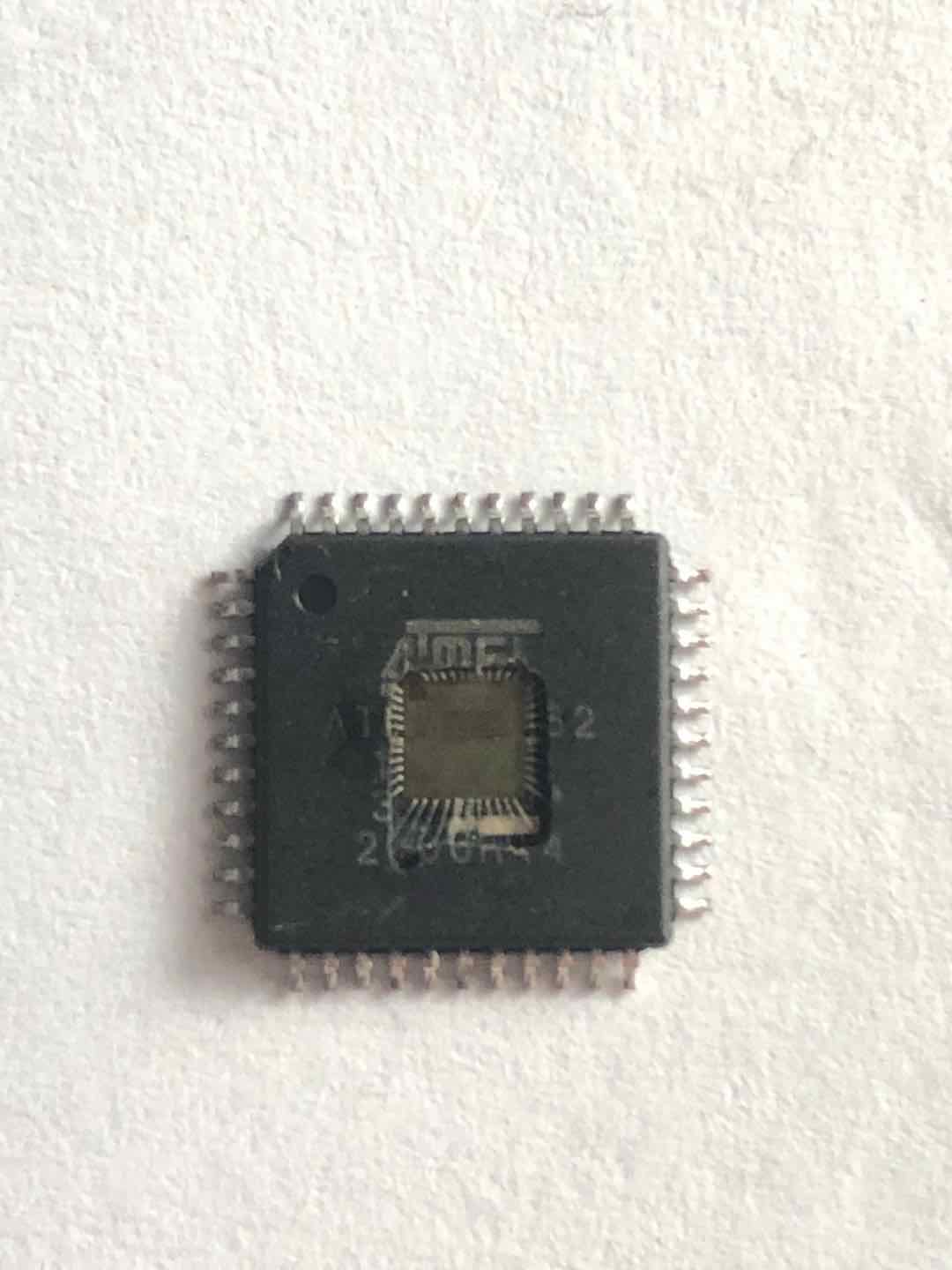
 Reverse Locked Microcontroller STM32F302RE Flash Program
Reverse Locked Microcontroller STM32F302RE Flash Program is dump embedded firmware of mcu stm32f302re out from its flash memory, copy secured mcu stm32f302re to new microcontroller;
- The POR monitors only the VDD supply voltage. During the startup phase it is required that VDDA should arrive first and be greater than or equal to VDD.
- The PDR monitors both the VDD and VDDA supply voltages, however the VDDA power supply supervisor can be disabled (by programming a dedicated Option bit) to reduce the power consumption if the application design ensures that VDDA is higher than or equal to VDD.
The device features an embedded programmable voltage detector (PVD) that monitors the VDD power supply and compares it to the VPVD threshold when restoring stm32f301r8 flash firmware from microcontroller. An interrupt can be generated when VDD drops below the VPVD threshold and/or when VDD is higher than the VPVD threshold.
The interrupt service routine can then generate a warning message and/or put the MCU into a safe state. The PVD is enabled by software.
reverso bloqueado microcontrolador STM32F302RE programa flash é dump firmware embutido de mcu stm32f302re para fora de sua memória flash, cópia segura mcu stm32f302re para o novo microcontrolador
The regulator has three operation modes: main (MR), low power (LPR), and power-down.
- The MR mode is used in the nominal regulation mode (Run)
- The LPR mode is used in Stop mode.
The power-down mode is used in Standby mode: the regulator output is in high impedance by breaking microprocessor stm32f301c8 flash memory, and the kernel circuitry is powered down thus inducing zero consumption.
The voltage regulator is always enabled after reset. It is disabled in Standby mode.
Reverse ARM STM32F031F4 Microprocessor Source Code
Reverse ARM STM32F031F4 Microprocessor Source Code from its flash memory, and copy flash firmware to new mcu stm32f031f4 by programmer, the locked bits of microcontroller stm32f031f4 has been disabled by mcu cracking technique;
The MCU is placed under the following conditions:
- VDD = VDDA = 3.3 V
- All I/O pins are in analog input configuration
- The Flash memory access time is adjusted to fHCLK frequency:
- 0 wait state and Prefetch OFF from 0 to 24 MHz
- 1 wait state and Prefetch ON above 24 MHz
- When the peripherals are enabled, fPCLK = fHCLK
- PLL is used for frequencies greater than 8 MHz
AHB prescaler of 2, 4, 8 and 16 is used for the frequencies 4 MHz, 2 MHz, 1 MHz and 500 kHz respectively.
The current consumption of the I/O system has two components: static and dynamic when recover flash firmware from stm32f031e6 arm microcontroller.
All the I/Os used as inputs with pull-up generate current consumption when the pin is externally held low. The value of this current consumption can be simply computed by using the pull-up/pull-down resistors values given in Table 46: I/O static characteristics.
обратный исходный код микропроцессора ARM STM32F031F4 из его флэш-памяти и копирование прошивки флэш-памяти на новый микроконтроллер STM32F031F4 с помощью программиста, заблокированные биты микроконтроллера STM32F031F4 были отключены методом взлома микроконтроллера;
For the output pins, any external pull-down or external load must also be considered to estimate the current consumption. Additional I/O current consumption is due to I/Os configured as inputs if an intermediate voltage level is externally applied by breaking arm microprocessor stm32f030cc flash memory.
This current consumption is caused by the input Schmitt trigger circuits used to discriminate the input value. Unless this specific configuration is required by the application, this supply current consumption can be avoided by configuring these I/Os in analog mode. This is notably the case of ADC input pins which should be configured as analog inputs.
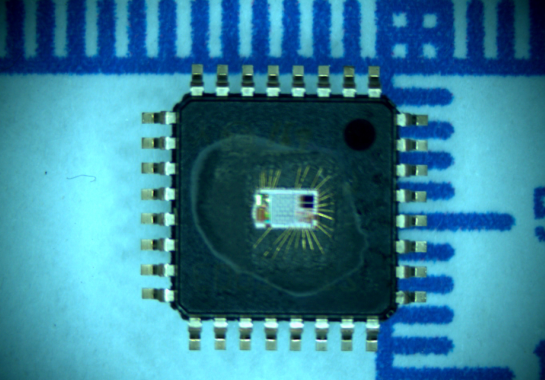
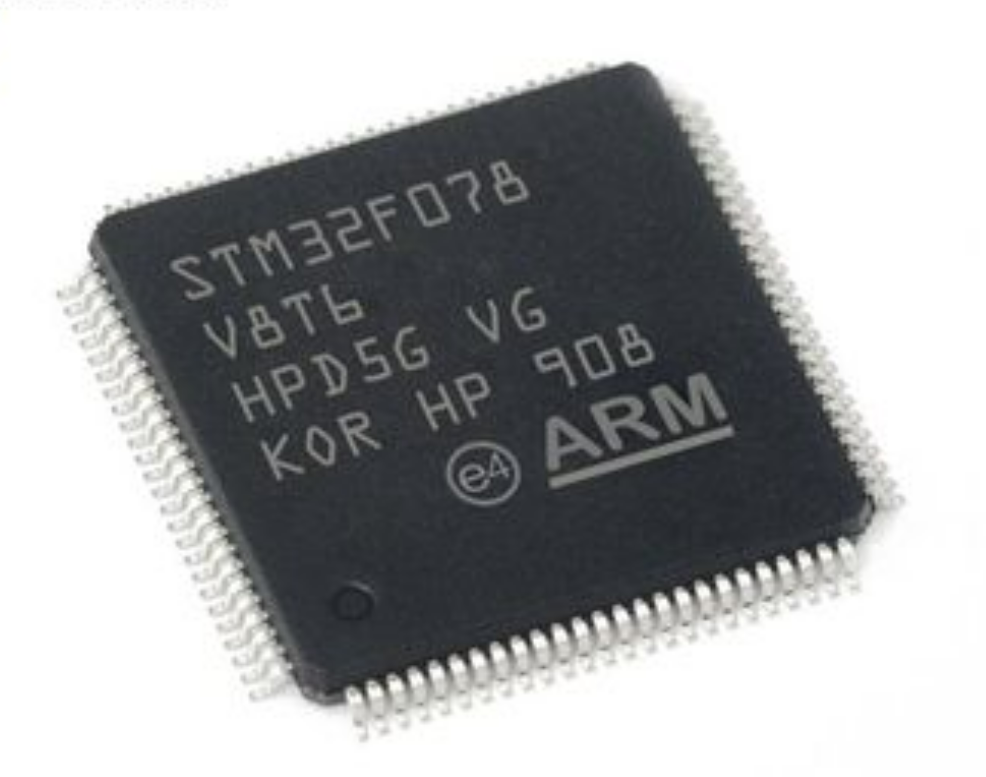
Reverse Engineering ARM STM32F078R8 MCU
Reverse Engineering ARM STM32F078R8 MCU process will help engineer to figure out how to crack stm32f078r8 microcontroller fuse bit by focus ion beam and then readout embedded heximal file from stm32f078r8 microprocessor’s flash memory;
The internal voltage reference (VREFINT) provides a stable (bandgap) voltage output for the ADC and comparators. VREFINT is internally connected to the ADC_IN17 input channel. The precise voltage of VREFINT is individually measured for each part by ST during production test and stored in the system memory area. It is accessible in read-only mode.
This embedded hardware feature allows the application to measure the VBAT battery voltage using the internal ADC channel ADC_IN18. As the VBAT voltage may be higher than VDDA after breaking stm32f071rb microcontroller locked bit, and thus outside the ADC input range, the VBAT pin is internally connected to a bridge divider by 2. As a consequence, the converted digital value is half the VBAT voltage.
El proceso de ingeniería inversa de MCU ARM STM32F078R8 ayudará al ingeniero a descubrir cómo descifrar el fusible del microcontrolador STM32F078R8 bit a haz de iones de enfoque y luego leer el archivo hexamal incrustado de la memoria flash del microprocesador STM32F078R8;
The two 12-bit buffered DAC channels can be used to convert digital signals into analog voltage signal outputs. The chosen design structure is composed of integrated resistor strings and an amplifier in non-inverting configuration.
This digital Interface supports the following features:
- 8-bit or 12-bit monotonic output
- Left or right data alignment in 12-bit mode
- Synchronized update capability
- Noise-wave generation
- Triangular-wave generation
- Dual DAC channel independent or simultaneous conversions
- DMA capability for each channel
- External triggers for conversion
Six DAC trigger inputs are used in the device. The DAC is triggered through the timer trigger outputs and the DAC interface is generating its own DMA requests to reverse stm32f071r8 arm microcomputer flash program.
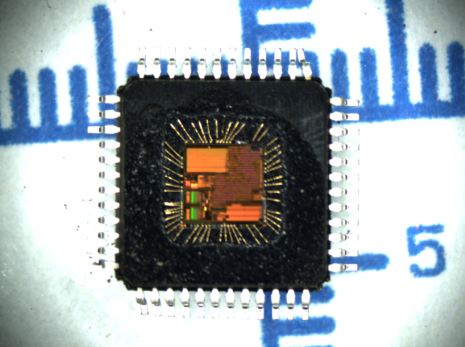
Reverse Engineer STM32F078VB Microcontroller Program
Reverse Engineer STM32F078VB Microcontroller Program actually is a process to clone a microprocessor stm32f078vb with the same heximal from its flash memory, original embedded firmware will be extracted from mcu stm32f078v8;
The Arm® Cortex®-M0 is a generation of Arm 32-bit RISC processors for embedded systems. It has been developed to provide a low-cost platform that meets the needs of MCU implementation, with a reduced pin count and low-power consumption, while delivering outstanding computational performance and an advanced system response to interrupts.
El programa de microcontrolador STM32F078VB de ingeniería inversa en realidad es un proceso para clonar un microprocesador STM32F078VB con el mismo hexamal de su memoria flash, el firmware integrado original se extraerá de MCU STM32F078V8;
The Arm® Cortex®-M0 processors feature exceptional code-efficiency, delivering the high performance expected from an Arm core, with memory sizes usually associated with 8- and 16-bit devices for stm32f071rb arm microcontroller memory locked bit breaking. The STM32F078CB/RB/VB devices embed Arm core and are compatible with all Arm tools and software.
The device has the following features:
- 16 Kbytes of embedded SRAM accessed (read/write) at CPU clock speed with 0 wait states and featuring embedded parity checking with exception generation for fail-critical applications.
- The non-volatile memory is divided into two arrays:
- 128 Kbytes of embedded Flash memory for programs and data
- Option bytes
- The non-volatile memory is divided into two arrays:
The option bytes are used to write-protect the memory (with 4 KB granularity) and/or readout-protect the whole memory with the following options:
- Level 0: no readout protection
- Level 1: memory readout protection, the Flash memory cannot be read from or written to if either debug features are connected or boot in RAM is selected which the stm32f071vb mcu flash memory can be hacked;
Level 2: chip readout protection, debug features (Arm® Cortex®-M0 serial wire) and boot in RAM selection disabled
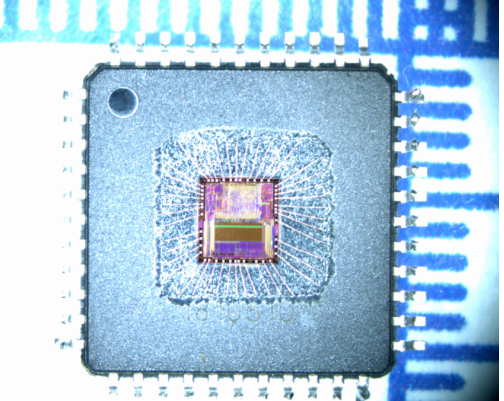
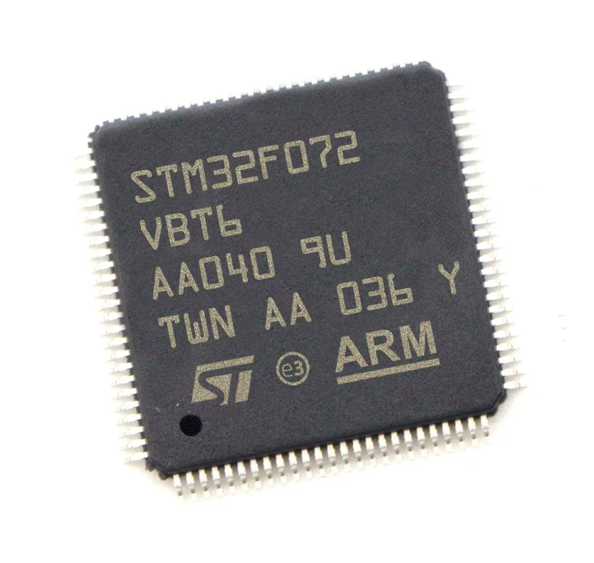
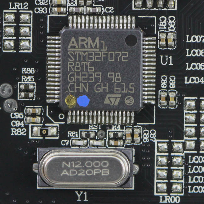
Reverse Engineering STM32F072VB Microcontroller Flash Program
Reverse Engineering STM32F072VB Microcontroller Flash Program is a process to extract embedded firmware from stm32f072vb flash memory, and then original mcu stm32f072vb microprocessor tamper resistance system will be cracked;
Each of the GPIO pins can be configured by software as output (push-pull or open-drain), as input (with or without pull-up or pull-down) or as peripheral alternate function. Most of the GPIO pins are shared with digital or analog alternate functions. The I/O configuration can be locked if needed following a specific sequence in order to avoid spurious writing to the I/Os registers.
The 7-channel general-purpose DMAs manage memory-to-memory, peripheral-to-memory and memory-to-peripheral transfers.
The DMA supports circular buffer management, removing the need for user code intervention when the controller reaches the end of the buffer and decrypt source code from arm microcontroller stm32f072v8.
reverse engineering Il programma flash del microcontrollore STM32F072VB è un processo per estrarre il firmware incorporato dalla memoria flash STM32F072VB, e quindi il sistema di resistenza alla manomissione del microprocessore MCU originale STM32F072VB verrà violato;
Each channel is connected to dedicated hardware DMA requests, with support for software trigger on each channel. Configuration is made by software and transfer sizes between source and destination are independent. DMA can be used with the main peripherals: SPIx, I2Sx, I2Cx, USARTx, all TIMx timers (except TIM14), DAC and ADC.
The STM32F0xx family embeds a nested vectored interrupt controller able to handle up to 32 maskable interrupt channels in order to hack stm32f071vb flash memory content (not including the 16 interrupt lines of Cortex®-M0) and 4 priority levels.
- Closely coupled NVIC gives low latency interrupt processing
- Interrupt entry vector table address passed directly to the core
- Closely coupled NVIC core interface
- Allows early processing of interrupts
- Processing of late arriving higher priority interrupts
- Support for tail-chaining
- Processor state automatically saved
- Interrupt entry restored on interrupt exit with no instruction overhead
This hardware block provides flexible interrupt management features with minimal interrupt latency.
Reverse Engineering ARM Microcontroller STM32F072R8 Flash Memory
Reverse Engineering ARM Microcontroller STM32F072R8 Flash Memory and readout embedded heximal file from stm32f072rb flash memory after crack microprocessor stm32f072rb locked bit by focus ion beam technique;
The device has the following features:
16 Kbytes of embedded SRAM accessed (read/write) at CPU clock speed with 0 wait states and featuring embedded parity checking with exception generation for fail-critical applications.
The non-volatile memory is divided into two arrays:
64 to 128 Kbytes of embedded Flash memory for programs and data when hack stm32f071vb mcu flash memory protection
Option bytes
The option bytes are used to write-protect the memory (with 4 KB granularity) and/or readout-protect the whole memory with the following options:
Level 0: no readout protection
reverse engineering microcontrollore ARM STM32F072R8 memoria flash e lettura file eshimale incorporato da STM32F072RB memoria flash dopo crack microprocessore STM32F072RB bit bloccato dalla tecnica del fascio ionico di messa a fuoco
Level 1: memory readout protection, the Flash memory cannot be read from or written to if either debug features are connected or boot in RAM is selected by breaking stm32f071rb microcontroller locked bit;
Level 2: chip readout protection, debug features (Arm® Cortex®-M0 serial wire) and boot in RAM selection disabled
At startup, the boot pin and boot selector option bit are used to select one of the three boot options:
boot from User Flash memory
boot from System Memory
boot from embedded SRAM
The boot loader is located in System Memory. It is used to reprogram the Flash memory by using USART on pins PA14/PA15, or PA9/PA10 or I2C on pins PB6/PB7 or through the USB DFU interface.
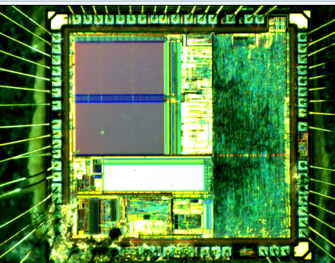
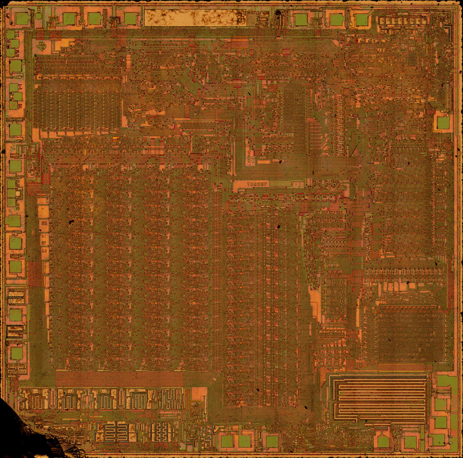
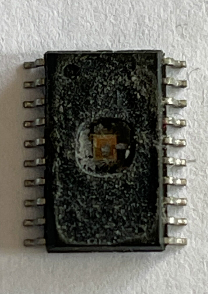
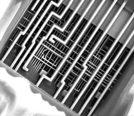
Arm Microprocessor STM32F072RB CPU Reverse Engineering
Arm Microprocessor STM32F072RB CPU Reverse Engineering starts from delayer the microcontroller structure one by one in the reverse order of MCU production, which is also called mcu stm32f072rb cracking, finally purpose of this execution is to have the embedded heximal file extracted from microprocessor stm32f072rb flash memory;
This datasheet provides characteristics and ordering information of the STM32F072x8/xB microcontrollers.
This document should be read in conjunction with the STM32F0xxxx reference manual (RM0091). The reference manual is available from the STMicroelectronics website www.st.com. For information on the Arm®(a)Cortex®-M0 core, please refer to the Arm® Cortex®-M0 Technical Reference Manual, available from the www.arm.com website.
The STM32F072x8/xB microcontrollers incorporate the high-performance Arm®Cortex®-M0 32-bit RISC core operating at up to 48 MHz frequency, high-speed embedded memories (up to 128 Kbytes of Flash memory and 16 Kbytes of SRAM), and an extensive range of enhanced peripherals and I/Os.
Il reverse engineering della CPU del microprocessore STM32F072RB inizia dal delayer della struttura del microcontrollore uno per uno nell’ordine inverso della produzione MCU, che è anche chiamato cracking MCU STM32F072RB, infine lo scopo di questa esecuzione è quello di avere il file exical incorporato estratto dalla memoria flash del microprocessore STM32F072RB;
All devices offer standard communication interfaces (two I2Cs, two SPI/I2S, one HDMI CEC and four USARTs), one USB Full-speed device (crystal-less), one CAN, one 12-bit ADC, one 12-bit DAC with two channels, seven 16-bit timers, one 32-bit timer and an advanced-control PWM timer.
The STM32F072x8/xB microcontrollers operate in the -40 to +85 °C and -40 to +105 °C temperature ranges, from a 2.0 to 3.6 V power supply. A comprehensive set of power-saving modes allows the design of low-power applications by decrypting source code of stm32f071v8 mcu flash memory.
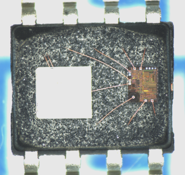
Reverse ARM Microcomputer STM32F071R8 Flash Program
Reverse ARM Microcomputer STM32F071R8 Flash Program is a process to crack arm mcu stm32f071r8 locked bit and disable the protection over its flash memory, after copying the extracted heximal to new processor stm32f071r8 for functions clones;

The current consumption of the on-chip peripherals is given in Table 35. The MCU is placed under the following conditions:
- All I/O pins are in analog mode
- All peripherals are disabled unless otherwise mentioned
- The given value is calculated by measuring the current consumption
- with all peripherals clocked off
- with only one peripheral clocked on
- Ambient operating temperature and supply voltage conditions summarized in Table 21: Voltage characteristics
The power consumption of the digital part of the on-chip peripherals is given in the process of arm microcontroller stm32f071vb source code decryption. The power consumption of the analog part of the peripherals (where applicable) is indicated in each related section of the datasheet.
In bypass mode the LSE oscillator is switched off and the input pin is a standard GPIO. The external clock signal has to respect the I/O characteristics in Section 6.3.14. However, the recommended clock input waveform is shown in Figure 15.
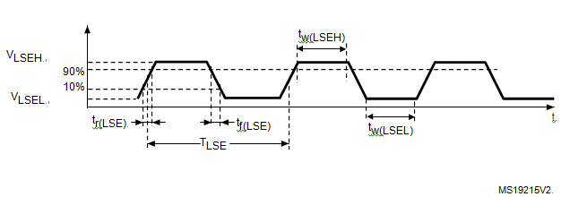
The high-speed external (HSE) clock can be supplied with a 4 to 32 MHz crystal/ceramic resonator oscillator. All the information given in this paragraph are based on design simulation results obtained with typical external components specified to hack stm32f071vb mcu flash memory binary.
Il reverse engineering della CPU del microprocessore STM32F072RB inizia dal delayer della struttura del microcontrollore uno per uno nell’ordine inverso della produzione MCU, che è anche chiamato cracking MCU STM32F072RB, infine lo scopo di questa esecuzione è quello di avere il file exical incorporato estratto dalla memoria flash del microprocessore STM32F072RB;
In the application, the resonator and the load capacitors have to be placed as close as possible to the oscillator pins in order to minimize output distortion and startup stabilization time. Refer to the crystal resonator manufacturer for more details on the resonator characteristics (frequency, package, accuracy).
Reverse Engineering Texas Instrument TMS320F28054PNQ Flash Memory
Reverse Engineering Texas Instrument TMS320F28054PNQ Flash Memory can help to locate the security fuse bit of MCU and crack dsp microcontroller tms320f28054 tamper resistance, and then extract embedded heximal from tms320f28054 flash memory;
The TI Reference Design Library is a robust reference design library spanning analog, embedded processor, and connectivity. Created by TI experts to help you jump start your system design, all reference designs include schematic or block diagrams, BOMs, and design files to speed your time to market. Search and download designs at the Select TI reference designs page.
Digitally Controlled Non-Isolated DC/DC Buck Converter Reference Design
This design implements a non-isolated DC/DC buck converter that is digitally controlled using a C2000 microcontroller. The main purpose of this design is to evaluate the powerSUITE Digital Power Software tools in the process of reversing secured dsp cpu tms320f28051 memory. The design consists of two separate boards: 1) Digital Power BoosterPack™ Plug-in Module and
2) C2000 F28069M LaunchPad™ Development Kit or C2000 F28377S LaunchPad Development Kit.
672W Highly Integrated Reference Design for Automotive Bidirectional 48V-12V Converter Today’s automotive power consumption is 3KW, which will increase to 10KW in the next 5 years.
A 12-V battery is unable to provide that much power. The 48-12V bidirectional convertor provides a high-power requirement solution with two phases, each capable of running 28 A. This solution allows bidirectional current control of both phases using a C2000 control stick and firmware OCP and OVP in order to attack dsp controller tms320f28053 flash memory.
The 48-12V bidirectional converter removes the voltage conditioner need and distributes loads more evenly. The 48-V battery is used to power high-torque motors and other high-power components, such as A/C compressors and EPS, with no change to 12-V battery loads.
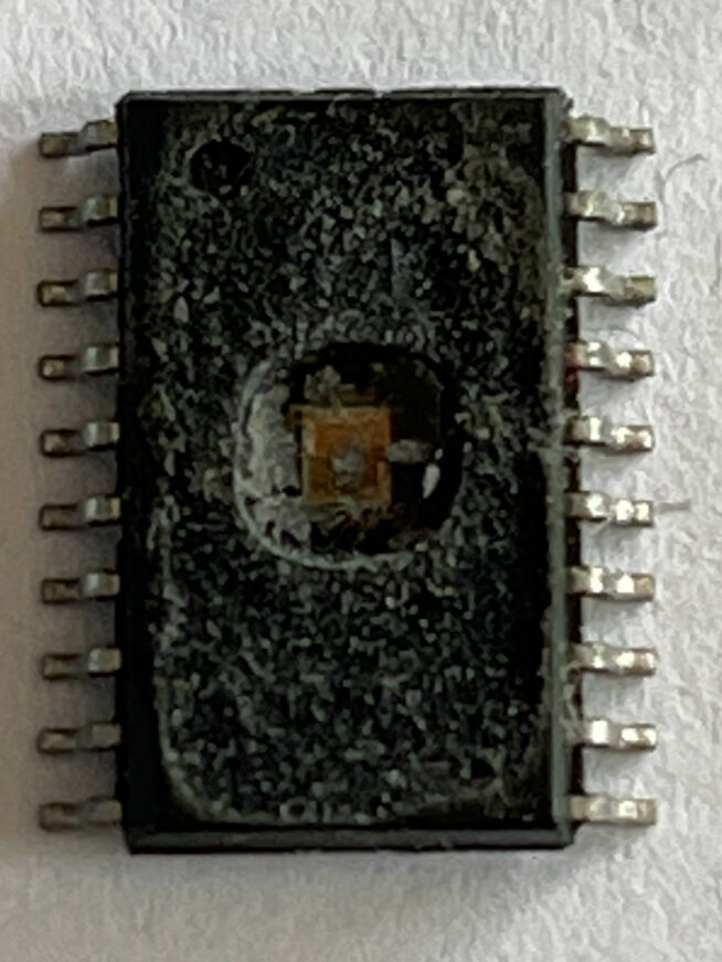
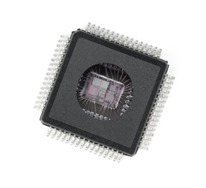
Reverse ST ST72F32AJ1 Microcontroller Flash Memory Binary
Reverse ST ST72F32AJ1 Microcontroller Flash Memory Binary needs to crack secured mcu st72f32aj1 flash memory fuse bit over the protection and copy embedded firmware from st72f32aj1 microprocessor;
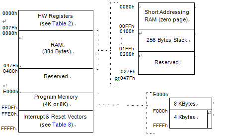
As shown in below Figure, the MCU is capable of ad- dressing 64K bytes of memories and I/O registers. The available memory locations consist of 128 bytes of register locations, up to 384 bytes of RAM and up to 8 Kbytes of user program memory by breaking st32f32ak1 mcu flash memory protection. The RAM space includes up to 256 bytes for the stack from 0100h to 01FFh.
The highest address bytes contain the user reset and interrupt vectors.
IMPORTANT: Memory locations marked as “Re- served” must never be accessed. Accessing a re- served area can have unpredictable effects on the device.
The contents of the I/O port DR registers are readable only in output configuration. In input configura- tion, the values of the I/O pins are returned instead of the DR register contents. The bits associated with unavailable pins must always keep their reset value.