Archive for the ‘Reverse Engineer Microcontroller’ Category
 Recover Microcontroller PIC16F874 Eeprom
Recover Microcontroller PIC16F874 Eeprom content needs to unlock mcu pic16f874 secured system and read the embedded firmware from mcu pic16f874 flash memory;
We can recover MICROCONTROLLER PIC16F874 Eeprom, please view the MICROCONTROLLER PIC16F874 Eeprom features for your reference:
This document contains device specific information
Additional information may be found in the PICmicro™ Mid-Range Reference Manual (DS33023), which may be obtained from your local Microchip Sales Representative or downloaded from the Microchip website before recover MICROCONTROLLER. The Reference Manual should be considered a complementary document to this data sheet, and is highly recommended recovering for a better understanding of the device architecture and operation of the peripheral modules.
There are four devices (PIC16F873, PIC16F874, PIC16F876 and PIC16F877) covered by this datasheet. The PIC16F876/873 devices come in 28-pin packages and the PIC16F877/874 devices come in 40-pin packages. The Parallel Slave Port is not implemented on the 28-pin devices before read avr atmel mcu firmware.
The following device block diagrams are sorted by pin number; 28-pin for Figure 1-1 and 40-pin for Figure 1-2.
The 28-pin and 40-pin pinouts are listed in Table 1-1 and Table 1-2, respectively. There are three memory blocks in each of the PIC16F87X MICROCONTROLLERs. The Program Memory and Data Memory have separate buses so that concurrent access can occur and is detailed in this section. The EEPROM data memory block is detailed in Section 4.0.
Additional information on device memory may be found in the PICmicro Mid-Range Reference Manual, (DS33023). The PIC16F87X devices have a 13-bit program counter capable of addressing an 8K x 14 program memory space if recover MICROCONTROLLER. The PIC16F877/876 devices have 8K x 14 words of FLASH program memory, and the PIC16F873/874 devices have 4K x 14. Accessing a location above the physically implemented address will cause a wraparound.
The RESET vector is at 0000h and the interrupt vector is at 0004h.
Recovery Microcontroller PIC16F872 Program
Recovery Microcontroller PIC16F872 Program including reading mcu pic16f872 eeprom and clone microchip pic16f872 protective flash memory;
Microcontroller Core Features:
· High-performance RISC CPU
· Only 35 single word instructions to learn
· All single cycle instructions except for program branches which are two cycle when Recovery MICROCONTROLLER
· Operating speed: DC – 20 MHz clock input DC – 200 ns instruction cycle
· 2K x 14 words of FLASH Program Memory 128 x 8 bytes of Data Memory (RAM) 64 x 8 bytes of EEPROM Data Memory
· Pinout compatible to the PIC16C72A
· Interrupt capability (up to 10 sources)
· Eight level deep hardware stack
· Direct, indirect and relative addressing modes
· Power-on Reset (POR)
· Power-up Timer (PWRT) and Oscillator Start-up Timer (OST)
· Watchdog Timer (WDT) with its own on-chip RC oscillator for reliable operation
· Programmable code-protection
· Power saving SLEEP mode
· Selectable oscillator options
· Low-power, high-speed CMOS FLASH/EEPROM technology
· In-Circuit Serial Programming (ICSP) via two pins
· Single 5V In-Circuit Serial Programming capability
· In-Circuit Debugging via two pins
· Processor read/write access to program memory
· Wide operating voltage range: 2.0V to 5.5V
· High Sink/Source Current: 25 mA
· Commercial and Industrial temperature ranges
· Low-power consumption:
– < 2 mA typical @ 5V, 4 MHz
– 20 µA typical @ 3V, 32 kHz
– < 1 µA typical standby current
Peripheral Features:
· Timer0: 8-bit timer/counter with 8-bit prescaler
· Timer1: 16-bit timer/counter with prescaler, can be incremented during sleep via external crystal/clock when Recovery MICROCONTROLLER
· Timer2: 8-bit timer/counter with 8-bit period register, prescaler and postscaler
· One Capture, Compare, PWM module
– Capture is 16-bit, max. resolution is 12.5 ns
– Compare is 16-bit, max. resolution is 200 ns
– PWM max. resolution is 10-bit
· 10-bit multi-channel Analog-to-Digital converter after Recovery MICROCONTROLLER
· Synchronous Serial Port (SSP) with SPI (Master Mode) and I2C (Master/Slave)
· Brown-out detection circuitry for Brown-out Reset (BOR)
There are three memory blocks in each of these PICmicro® MICROCONTROLLERs. The Program Memory and Data Memory have separate buses, so that concurrent access can occur, and is detailed in this section. The EEPROM data memory block is detailed in Section 4.0. Additional information on device memory may be found in the PICmicro Mid-Range Reference Manual, (DS33023) if Recovery MICROCONTROLLER.
Recovery MCU PIC16C662 Heximal
Recovery MCU PIC16C662 Heximal
We can Recovery MCU PIC16C662 Heximal, please view the MCU PIC16C662 features for your reference:
The clock input (from OSC1) is internally divided by four to generate four non-overlapping quadrature clocks namely Q1, Q2, Q3, and Q4. Internally, the program counter (PC) is incremented every Q1, the instruction is fetched from the program memory and latched into the instruction register in Q4. The instruction is decoded and executed during the following Q1 through Q4. The clocks and instruction execution flow is shown in Figure 3-3 if Recovery MCU.
An “Instruction Cycle” consists of four Q cycles (Q1, Q2, Q3, and Q4). The instruction fetch and execute are pipelined such that fetch takes one instruction cycle while decode and execute takes another instruction cycle. However, due to the pipelining, each instruction effectively executes in one cycle after Recovery MCU.
If an instruction causes the program counter to change (e.g., GOTO) then two cycles are required to complete the instruction (Example 3-1). A fetch cycle begins with the program counter (PC) incrementing in Q1 before Recovery MCU.
In the execution cycle, the fetched instruction is latched into the “Instruction Register (IR)” in cycle Q1. This instruction is then decoded and executed during the Q2, Q3, and Q4 cycles. Data memory is read during Q2 (operand read) and written during Q4 (destination write) if Recovery MCU.
The PIC16C64X & PIC16C66X have a 13-bit program counter capable of addressing an 8K x 14 program memory space. For the PIC16C641 and PIC16C661 only the first 2K x 14 (0000h – 07FFh) is physically implemented. For the PIC16C642 and PIC16C662 only the first 4K x 14 (0000h – 0FFh) is physically implemented before Recovery MCU.
Accessing a location above the 2K or 4K boundary will cause a wrap-around. The reset vector is at 0000h and the interrupt vector is at 0004h (Figure 4- 1 and Figure 4-2). See Section 4.4 for Program Memory paging. The data memory (Figure 4-4) is partitioned into two banks which contain the general purpose registers and the special function registers when Recovery MCU.
Bank 0 is selected when bit RP0 (STATUS<5>) is cleared. Bank 1 is selected when the RP0 bit is set. The Special Function Registers are located in the first 32 locations of each Bank before Recovery MCU.
Register locations A0h-EFh (Bank 1) are general purpose registers implemented as static RAM. Some special function registers are mapped in Bank 1. The register file is organized as 176 x 8 for the PIC16C642/662, and 128 x8 for the PIC16C641/661. Each is accessed either directly, or indirectly through the File Select Register FSR (Section 4.5) if Recovery MCU.
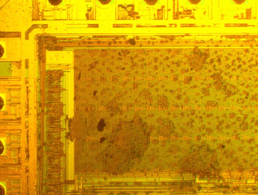
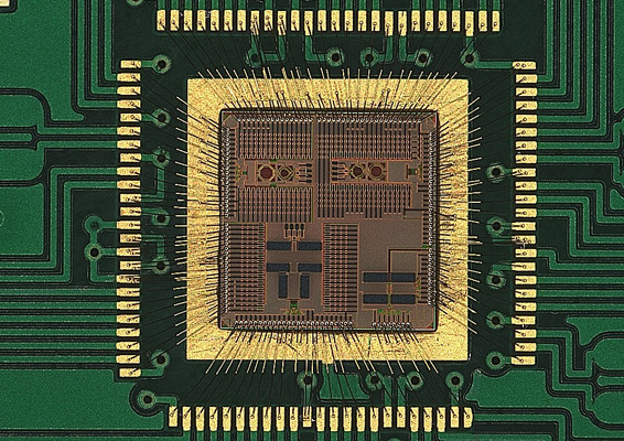
Reverse Engineering Microcontroller PIC16C716 Heximal
Reverse engineering Microcontroller PIC16C716 can locate the security fuse bit of it, and break off it in order to take the embedded software from mcu pic16c716, and then copy the microprocessor pic16c716 program out to new MCU;
Reverse engineering Microcontroller PIC16C716 can locate the security fuse bit of it, and break off it in order to take the embedded software from mcu pic16c716, and then copy the microprocessor pic16c716 program out to new MCU
There are two memory blocks in each of these PICmicro® microcontroller devices. Each block (Program Memory and Data Memory) has its own bus so that concurrent access can occur.
Additional information on device memory may be found in the PICmicro Mid-Range Reference Manual, (DS33023).
The PIC16C712/716 has a 13-bit program counter capable of addressing an 8K x 14 program memory space. PIC16C712 has 1K x 14 words of program memory and PIC16C716 has 2K x 14 words of program memory. Accessing a location above the physically implemented address will cause a wraparound.
The reset vector is at 0000h and the interrupt vector is at 0004h.
Each bank extends up to 7Fh (128 bytes). The lower locations of each bank are reserved for the Special
Function Registers. Above the Special Function Registers are General Purpose Registers, implemented as static RAM. All implemented banks contain special function registers. Some “high use” special function registers from one bank may be mirrored in another bank for code reduction and quicker access.
The Special Function Registers are registers used by the CPU and Peripheral Modules for controlling the desired operation of the device. These registers are implemented as static RAM. A list of these registers is give in Table 2-1 after attacking Microcontroller.
The special function registers can be classified into two sets; core (CPU) and peripheral. Those registers associated with the core functions are described in detail in this section. Those related to the operation of the peripheral features are described in detail in that peripheral feature section.
cracking secured mcu PIC16C716 flash memory and readout embedded flash memory binary and heximal file
The STATUS register, shown in Figure 2-4, contains the arithmetic status of the ALU, the RESET status and the bank select bits for data memory. The STATUS register can be the destination for any instruction, as with any other register. If the STATUS register is the destination for an instruction that affects the Z, DC or C bits, then the write to these three bits is disabled. These bits are set or cleared according to the device logic. Furthermore, the TO and PD bits are not writable. Therefore, the result of an instruction with the STATUS register as destination may be different than intended.
The program counter (PC) specifies the address of the instruction to fetch for execution. The PC is 13 bits wide. The low byte is called the PCL register after Reverse engineering Microcontroller. This register is readable and writable. The high byte is called the PCH register. This register contains the PC<12:8> bits and is not directly readable or writable. All updates to the PCH register go through the PCLATH register.
The stack allows a combination of up to 8 program calls and interrupts to occur. The stack contains the return address from this branch in program execution. Midrange devices have an 8 level deep x 13-bit wide hardware stack. The stack space is not part of either program or data space and the stack pointer is not readable or writable. The PC is PUSHed onto the stack when a CALL instruction is executed or an interrupt causes a branch. The stack is POPed in the event of a RETURN, RETLW or a RETFIE instruction execution when Reverse engineering Microcontroller.
PCLATH is not modified when the stack is PUSHed or POPed. After the stack has been PUSHed eight times, the ninth push overwrites the value that was stored from the first push. The tenth push overwrites the second push (and so on). The CALL and GOTO instructions provide 11 bits of address to allow branching within any 2K program memory page. When doing a CALL or GOTO instruction, the upper bit of the address is provided by PCLATH<3>.
unlock encrypted microcontroller pic16c716 flash memory and extract embedded firmware in the format of binary or heximal
When doing a CALL or GOTO instruction, the user must ensure that the page select bit is programmed so that the desired program memory page is addressed. If a return from a CALL instruction (or interrupt) is executed, the entire 13-bit PC is pushed onto the stack. Therefore, manipulation of the PCLATH<3> bit is not required for the return instructions (which POPs the address from the stack).
For example, CLRF STATUS will clear the upper-three bits and set the Z bit. This leaves the STATUS register as 000u u1uu (where u = unchanged).
Reverse Engineering Microcontroller ATmega128P Binary
Reverse Engineering Microcontroller ATmega128P to research its internal structure of circuitry pattern, through which we can find the location of security fuse bit and disable it by microcontroller cracking, and extract binary from memory;
Reverse Engineering Microcontroller ATmega128P to research its internal structure of circuitry pattern, through which we can find the location of security fuse bit and disable it by microcontroller cracking, and extract binary from memory
In non-PWM Waveform Generation modes, the match output of the comparator can be forced by writing a one to the Force Output Compare (FOCnx) bit.
Forcing compare match will not set the OCFnx Flag or reload/clear the timer, but the OCnx pin will be updated as if a real compare match had occurred (the COMn1:0 bits settings define whether the OCnx pin is set, cleared or toggled) when break Microcontroller atmega1280a binary.
All CPU writes to the TCNTn Register will block any compare match that occurs in the next timer clock cycle, even when the timer is stopped. This feature allows OCRnx to be initialized to the same value as TCNTn without triggering an interrupt when the Timer/Counter clock is enabled.
Since writing TCNTn in any mode of operation will block all compare matches for one timer clock cycle, there are risks involved when changing TCNTn when using any of the Output Compare channels, independent of whether the Timer/Counter is running or not before break Microcontroller atmega48p flash.
If the value written to TCNTn equals the OCRnx value, the compare match will be missed, resulting in incorrect waveform generation. Do not write the TCNTn equal to TOP in PWM modes with variable TOP values.
break atmega128 microcomputer and readout heximal program of mcu atmega128pa
The compare match for the TOP will be ignored and the counter will continue to 0xFFFF. Similarly, do not write the TCNTn value equal to BOTTOM when the counter is downcounting.
The setup of the OCnx should be performed before setting the Data Direction Register for the port pin to output. The easiest way of setting the OCnx value is to use the Force Output Compare (FOCnx) strobe bits in Normal mode. The OCnx Register keeps its value even when changing between Waveform Generation modes.
Be aware that the COMnx1:0 bits are not double buffered together with the compare value. Changing the COMnx1:0 bits will take effect immediately.
The Compare Output mode (COMnx1:0) bits have two functions. The Waveform Generator uses the COMnx1:0 bits for defining the Output Compare (OCnx) state at the next compare match. Secondly the COMnx1:0 bits control the OCnx pin output source before Recover Microcontroller atmega88pv firmware.
restoring atmega128p microcontroller program of heximal and extract firmware from flash memory
The I/O Registers, I/O bits, and I/O pins in the figure are shown in bold. Only the parts of the general I/O Port Control Registers (DDR and PORT) that are affected by the COMnx1:0 bits are shown. When referring to the OCnx state, the reference is for the internal OCnx Register, not the OCnx pin. If a system reset occur, the OCnx Register is reset to “0”.
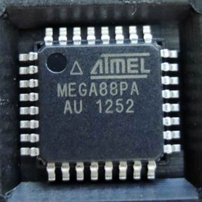
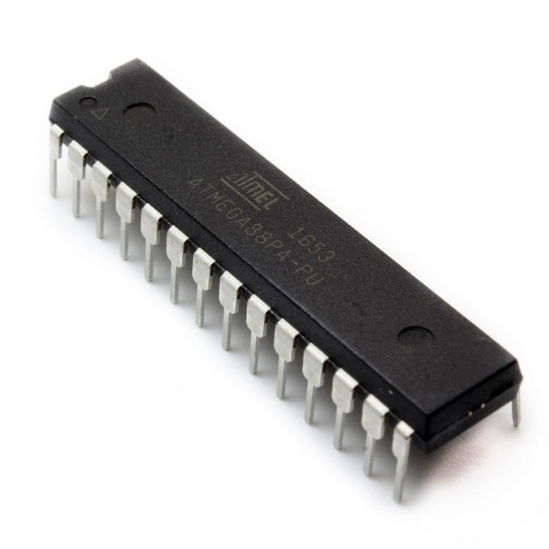
Break Microprocessor ATmega88PA Firmware
Break Microprocessor ATmega88PA and unlock protected mcu atmega88pa tamper resistance system, extract Firmware from microcontroller atmega88pa flash memoy;
The 16-bit comparator continuously compares TCNTn with the Output Compare Register (OCRnx). If TCNT equals OCRnx the comparator signals a match. A match will set the Output Compare Flag (OCFnx) at the next timer clock cycle. If enabled (OCIEnx =1), the Output Compare Flag generates an Output Compare interrupt.
The OCFnx Flag is automatically cleared when the interrupt is executed. Alternatively the OCFnx Flag can be cleared by software by writing a logical one to its I/O bit location. The Waveform Generator uses the match signal to generate an output according to operating mode set by the Waveform Generation mode (WGMn3:0) bits and Compare Output mode (COMnx1:0) bits.
The TOP and BOTTOM signals are used by the Waveform Generator for handling the special cases of the extreme values in some modes of operation (See“Modes of Operation” on page 147.)
A special feature of Output Compare unit A allows it to define the Timer/Counter TOP value (i.e., counter resolution). In addition to the counter resolution, the TOP value defines the period time for waveforms generated by the Waveform Generator before break atmel atmega48pv microprocessor memory.
Figure 52 shows a block diagram of the Output Compare unit. The small “n” in the register and bit names indicates the device number (n = n for Timer/Counter n), and the “x” indicates Output Compare unit (A/B/C). The elements of the block diagram that are not directly a part of the Output Compare unit are gray shaded.
crack atmega88pa microprocessor protection and extract heximal file from flash memory of mcu mega88pa
The OCRnx Register is double buffered when using any of the twelve Pulse Width Modulation (PWM) modes. For the Normal and Clear Timer on Compare (CTC) modes of operation, the double buffering is disabled. The double buffering synchronizes the update of the OCRnx Compare Register to either TOP or BOTTOM of the counting sequence.
The synchronization prevents the occurrence of odd-length, non-symmetrical PWM pulses, thereby making the output glitch-free.
The OCRnx Register access may seem complex, but this is not case. When the double buffering is enabled, the CPU has access to the OCRnx Buffer Register, and if double buffering is disabled the CPU will access the OCRnx directly if read ht68f4 microprocessor firmware.
The content of the OCR1x (Buffer or Compare) Register is only changed by a write operation (the Timer/Counter does not update this register automatically as the TCNT1 and ICR1 Register). Therefore OCR1x is not read via the high byte temporary register (TEMP). However, it is a good practice to read the low byte first as when accessing other 16-bit registers.
break atmega88pa microprocessor
Writing the OCRnx Registers must be done via the TEMP Register since the compare of all 16 bits is done continuously. The high byte (OCRnxH) has to be written first. When the high byte I/O location is written by the CPU, the TEMP Register will be updated by the value written. Then when the low byte (OCRnxL) is written to the lower eight bits, the high byte will be copied into the upper 8-bits of either the OCRnx buffer or OCRnx Compare Register in the same system clock cycle.
Break Microprocessor ATMEGA48P Flash
We can Break Microprocessor ATMEGA48P Flash, please view the Microprocessor ATMEGA48P features for your reference:
The Timer/Counter can be clocked by an internal or an external clock source. The clock source is selected by the Clock Select logic which is controlled by the Clock Select (CSn2:0) bits located in the Timer/Counter control Register B (TCCRnB) when break microprocessor flash.
The main part of the 16-bit Timer/Counter is the programmable 16-bit bi-directional counter unit. Figure 50 shows a block diagram of the counter and its surroundings if break microprocessor flash.
The 16-bit counter is mapped into two 8-bit I/O memory locations: Counter High (TCNTnH) containing the upper eight bits of the counter, and Counter Low (TCNTnL) containing the lower eight bits. The TCNTnH Register can only be indirectly accessed by the CPU before break microprocessor flash.
When the CPU does an access to the TCNTnH I/O location, the CPU accesses the high byte temporary register (TEMP). The temporary register is updated with the TCNTnH value when the TCNTnL is read, and TCNTnH is updated with the temporary register value when TCNTnL is written after break microprocessor flash.
This allows the CPU to read or write the entire 16-bit counter value within one clock cycle via the 8-bit data bus. It is important to notice that there are special cases of writing to the TCNTn Register when the counter is counting that will give unpredictable results when break microprocessor flash.
The special cases are described in the sections where they are of importance. Depending on the mode of operation used, the counter is cleared, incremented, or decremented at each timer clock (clkTn) if break microprocessor flash.
The clkTn can be generated from an external or internal clock source, selected by the Clock Select bits (CSn2:0). When no clock source is selected (CSn2:0 = 0) the timer is stopped. However, the TCNTn value can be accessed by the CPU, independent of whether clkTn is present or not before break microprocessor flash.
A CPU write overrides (has priority over) all counter clear or count operations. The counting sequence is determined by the setting of the Waveform Generation mode bits (WGMn3:0) located in the Timer/Counter Control Registers A and B (TCCRnA and TCCRnB) after break microprocessor flash.
There are close connections between how the counter behaves (counts) and how waveforms are generated on the Output Compare outputs OCnx. For more details about advanced counting sequences and waveform generation, see “Modes of Operation” on page 147 when break microprocessor flash.
The Timer/Counter Overflow Flag (TOVn) is set according to the mode of operation selected by the WGMn3:0 bits. TOVn can be used for generating a CPU interrupt if break microprocessor flash.
The Timer/Counter incorporates an input capture unit that can capture external events and give them a time-stamp indicating time of occurrence before break microprocessor flash.
The external signal indicating an event, or multiple events, can be applied via the ICPn pin or alternatively, for the Timer/Counter1 only, via the Analog Comparator unit. The time-stamps can then be used to calculate frequency, duty-cycle, and other features of the signal applied. Alternatively the time-stamps can be used for creating a log of the events after break microprocessor flash.
The Input Capture unit is illustrated by the block diagram shown in Figure 51. The elements of the block diagram that are not directly a part of the input capture unit are gray shaded. The small “n” in register and bit names indicates the Timer/Counter number.
Reverse Engineering PLD GAL16V8 Software
We can Reverse Engineering PLD GAL16V8 Software after break gal16v8 pld memory fuse bit and readout its jed file;
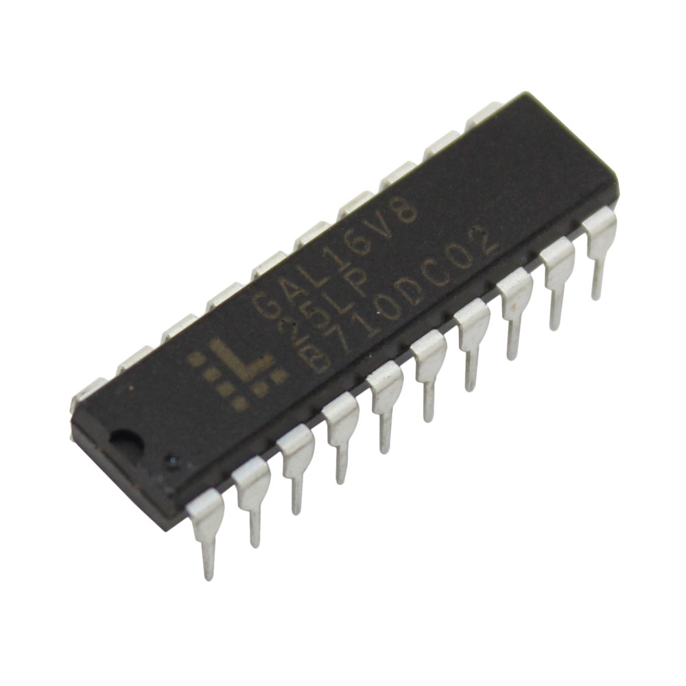
crack pld gal16v8 fuse bit and dump its embedded pof or jed file from memory
The Output Compare Register B contains an 8-bit value that is continuously compared with the counter value (TCNT0). A match can be used to generate an Output Compare interrupt, or to generate a waveform output on the OC0B pin.
Bit 2 – OCF0B: Timer/Counter 0 Output Compare B Match Flag
The OCF0B bit is set when a Compare Match occurs between the Timer/Counter and the data in OCR0B – Output Compare Register0 B. OCF0B is cleared by hardware when executing the corresponding interrupt handling vector.
Alternatively, OCF0B is cleared by writing a logic one to the flag. When the I-bit in SREG, OCIE0B (Timer/Counter Compare B Match Interrupt Enable), and OCF0B are set, the Timer/Counter Compare Match Interrupt is executed.
Bit 1 – OCF0A: Timer/Counter 0 Output Compare A Match Flag
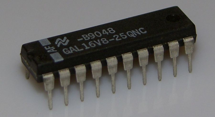
Reverse Engineering PLD GAL16V8 Software
The OCF0A bit is set when a Compare Match occurs between the Timer/Counter0 and the data in OCR0A – Output Compare Register0. OCF0A is cleared by hardware when executing the corresponding interrupt handling vector.
Alternatively, OCF0A is cleared by writing a logic one to the flag. When the I-bit in SREG, OCIE0A (Timer/Counter0 Compare Match Interrupt Enable), and OCF0A are set, the Timer/Counter0 Compare Match Interrupt is executed.
Bit 0 – TOV0: Timer/Counter0 Overflow Flag
The bit TOV0 is set when an overflow occurs in Timer/Counter0. TOV0 is cleared by hardware when executing the corresponding interrupt handling vector.
Alternatively, TOV0 is cleared by writing a logic one to the flag. When the SREG I-bit, TOIE0 (Timer/Counter0 Overflow Interrupt Enable), and TOV0 are set, the Timer/Counter0 Overflow interrupt is executed. The setting of this flag is dependent of the WGM02:0 bit setting. Refer to Table 76, “Waveform Generation Mode Bit Description” on page 130.
Recover MCU ATmega1280P Eeprom
Recover MCU ATmega1280P Eeprom content as well as flash program in the format of binary or heximal and copy the firmware to new microcontroller atmega1280p;
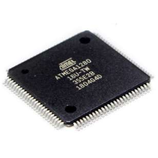
Recover MCU ATmega1280P Eeprom content as well as flash program in the format of binary or heximal and copy the firmware to new microcontroller atmega1280p;
The N variable represents the prescale factor (1, 8, 64, 256, or 1024). The extreme values for the OCR0A Register represent special cases when generating a PWM waveform output in the phase correct PWM mode. If the OCR0A is set equal to BOTTOM, the output will be continuously low and if set equal to MAX the output will be continuously high for non-inverted PWM mode. For inverted PWM the output will have the opposite logic values.
crack atmega1280p microprocessor fuse bit and readout embedded firmware from flash memory and eeprom memory
At the very start of period 2 in Figure 44 OCnx has a transition from high to low even though there is no Compare Match. The point of this transition is to guarantee symmetry around BOTTOM. There are two cases that give a transition without Compare Match. OCR0A changes its value from MAX, like in Figure 44. When the OCR0A value is MAX the OCn pin value is the same as the result of a down-counting Compare Match.
To ensure symmetry around BOTTOM the OCn value at MAX must correspond to the result of an up-counting Compare Match. The timer starts counting from a value higher than the one in OCR0A, and for that reason misses the Compare Match and hence the OCn change that would have happened on the way up. The Timer/Counter is a synchronous design and the timer clock (clkT0) is therefore shown as a clock enable signal in the following figures. The figures include information on when Interrupt Flags are set. Figure 45 contains timing data for basic Timer/Counter operation.
The figure shows the count sequence close to the MAX value in all modes other than phase correct PWM mode. These bits control the Output Compare pin (OC0B) behavior to recover atmega1280 mcu embedded heximal file. If one or both of the COM0B1:0 bits are set, the OC0B output overrides the normal port functionality of the I/O pin it is connected.
However, note that the Data Direction Register (DDR) bit corresponding to the OC0B pin must be set in order to enable the output driver. When OC0B is connected to the pin, the function of the COM0B1:0 bits depends on the WGM02:0 bit setting. Table 70 shows the COM0A1:0 bit functionality when the WGM02:0 bits are set to a normal or CTC mode (non-PWM).
Combined with the WGM02 bit found in the TCCR0B Register, these bits control the counting sequence of the counter, the source for maximum (TOP) counter value, and what type of waveform generation to be used. Modes of operation supported by the Timer/Counter unit are: Normal mode (counter), Clear Timer on Compare Match (CTC) mode, and two types of Pulse Width Modulation (PWM) modes.
Reverse Engineering MCU ATmega1284V Heximal
Reverse Engineering MCU ATmega1284V by unlock microcontroller ATmega1284V protective system, and readout heximal from microprocessor program memory, rewrite to the firmware to new ATmega1284V;
Reverse Engineering MCU ATmega1284V by unlock microcontroller ATmega1284V protective system, and readout heximal from microprocessor program memory, rewrite to the firmware to new ATmega1284V
The 8-bit comparator continuously compares TCNT0 with the Output Compare Registers (OCR0A and OCR0B). Whenever TCNT0 equals OCR0A or OCR0B, the comparator signals a match. A match will set the Output Compare Flag (OCF0A or OCF0B) at the next timer clock cycle. If the corresponding interrupt is enabled, the Output Compare Flag generates an Output Compare interrupt if attacking PIC16F506 MCU code.
The Output Compare Flag is automatically cleared when the interrupt is executed. Alternatively, the flag can be cleared by software by writing a logical one to its I/O bit location. The Waveform Generator uses the match signal to generate an output according to operating mode set by the WGM02:0 bits and Compare Output mode (COM0x1:0) bits after copy microcontroller PIC16F747 code.
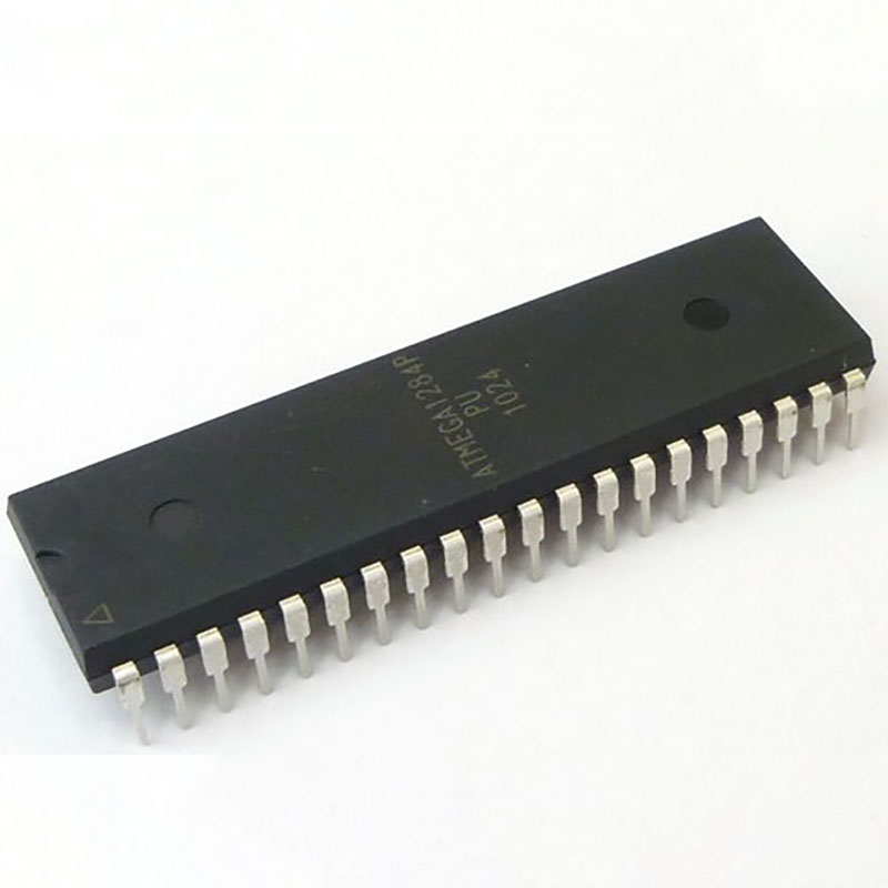
unlock ATMEGA1284P secured mcu fuse bit and extract embedded flash heximal file and eeprom binary program
The max and bottom signals are used by the Waveform Generator for handling the special cases of the extreme values in some modes of operation (“Modes of Operation” on page 121). Figure 40 shows a block diagram of the Output Compare unit. The OCR0x Registers are double buffered when using any of the Pulse Width Modulation (PWM) modes.
For the normal and Clear Timer on Compare (CTC) modes of operation, the double buffering is disabled. The double buffering synchronizes the update of the OCR0x Compare Registers to either top or bottom of the counting sequence.
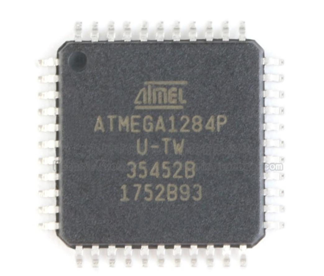
decrypt protected ATMEGA1284P controller and readout its flash firmware
The synchronization prevents the occurrence of odd-length, non-symmetrical PWM pulses, thereby making the output glitch-free. The OCR0x Register access may seem complex, but this is not case. When the double buffering is enabled, the CPU has access to the OCR0x Buffer Register, and if double buffering is disabled the CPU will access the OCR0x directly.