Archive for the ‘Reverse Engineer Microcontroller’ Category
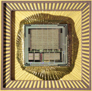
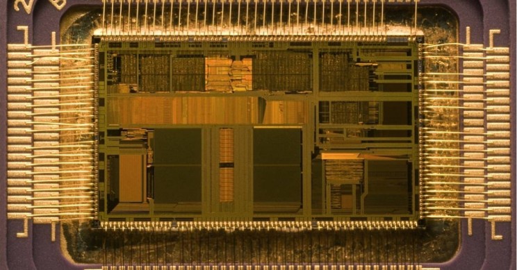
 Copy IC ATmega162 Binary
Copy IC ATmega162 Binary content and unlock avr atmega162 mcu protection, and extract the embedded firmware from microcontroller atmega162 flash and eeprom memory;
High-performance, Low-power AVR® 8-bit Microcontroller
· Advanced RISC Architecture
– 131 Powerful Instructions – Most Single-clock Cycle Execution
– 32 x 8 General Purpose Working Registers
– Fully Static Operation
– Up to 16 MIPS Throughput at 16 MHz
– On-chip 2-cycle Multiplier
High Endurance Non-volatile Memory segments
– 16K Bytes of In-System Self-programmable Flash program memory
– 512 Bytes EEPROM
– 1K Bytes Internal SRAM
– Write/Erase cycles: 10,000 Flash/100,000 EEPROM
– Data retention: 20 years at 85°C/100 years at 25°C(1)
– Optional Boot Code Section with Independent Lock Bits
In-System Programming by On-chip Boot Program
True Read-While-Write Operation
– Up to 64K Bytes Optional External Memory Space
8-bit Microcontroller
with 16K Bytes
In-System– Programming Lock for Software Security
JTAG (IEEE std. 1149.1 Compliant) Interface
– Boundary-scan Capabilities According to the JTAG Standard
– Extensive On-chip Debug Support
– Programming of Flash, EEPROM, Fuses, and Lock Bits through the JTAG Interface
Peripheral Features
– Two 8-bit Timer/Counters with Separate Prescalers and Compare Modes
– Two 16-bit Timer/Counters with Separate Prescalers, Compare Modes, and
Capture Modes
– Real Time Counter with Separate Oscillator
– Six PWM Channels
– Dual Programmable Serial USARTs
– Master/Slave SPI Serial Interface
– Programmable Watchdog Timer with Separate On-chip Oscillator before Copy IC
– On-chip Analog Comparator
Special Microcontroller Features
– Power-on Reset and Programmable Brown-out Detection
– Internal Calibrated RC Oscillator
– External and Internal Interrupt Sources
– Five Sleep Modes: Idle, Power-save, Power-down, Standby, and Extended Standby
I/O and Packages
– 35 Programmable I/O Lines
– 40-pin PDIP, 44-lead TQFP, and 44-pad MLF
Operating Voltages
– 1.8 – 5.5V for ATmega162V
– 2.7 – 5.5V for ATmega162
Speed Grades
– 0 – 8 MHz for ATmega162V
– 0 – 16 MHz for ATmega162
Programmable Flash when BREAK IC
Break Microcontroller ATtiny24 Code
Break Microcontroller ATtiny24 is a process to unlock mcu attiny24’s fuse bit and then extract code from microprocessor attiny24 flash and eeprom memory for MCU cloning;
Features
High Performance, Low Power AVR® 8-Bit Microcontroller
Advanced RISC Architecture
– 120 Powerful Instructions – Most Single Clock Cycle Execution
– 32 x 8 General Purpose Working Registers
– Fully StatMicrocontroller Operation
Non-volatile Program and Data Memories
– 2/4/8K Byte of In-System Programmable Program Memory Flash (ATtiny24/44/84)
Endurance: 10,000 Write/Erase Cycles
– 128/256/512 Bytes In-System Programmable EEPROM (ATtiny24/44/84)
Endurance: 100,000 Write/Erase Cycles
– 128/256/512 Bytes Internal SRAM (ATtiny24/44/84)
– Programming Lock for Self-Programming Flash Program and EEPROM Data Security before decrypt ic flash memory
Peripheral Features
– Two Timer/Counters, 8- and 16-bit counters with two PWM Channels on both
– 10-bit ADC
8 single-ended channels
12 differential ADC channel pairs with programmable gain (1x, 20x) Temperature Measurement
– Programmable Watchdog Timer with Separate On-chip Oscillator
– On-chip Analog Comparator
– Universal Serial Interface
Special MMicrocontrollerrocontroller Features
– debugWIRE On-chip Debug System
– In-System Programmable via SPI Port
– External and Internal Interrupt Sources
– Pin Change Interrupt on 12 pins
– Low Power Idle, ADC Noise Reduction, Standby and Power-down Modes
– Enhanced Power-on Reset Circuit
– Programmable Brown-out Detection Circuit
– Internal Calibrated Oscillator
– On-chip Temperature Sensor I/O and Packages
– 14-pin SOMICROCONTROLLER, PDIP and 20-pin QFN/MLF: Twelve Programmable I/O Lines
Operating Voltage:
– 1.8 – 5.5V for ATtiny24V/44V/84V
– 2.7 – 5.5V for ATtiny24/44/84
Speed Grade
– ATtiny24V/44V/84V: 0 – 4 MHz @ 1.8 – 5.5V, 0 – 10 MHz @ 2.7 – 5.5V
– ATtiny24/44/84: 0 – 10 MHz @ 2.7 – 5.5V, 0 – 20 MHz @ 4.5 – 5.5V
Industrial Temperature Range
Low Power Consumption
Preliminary Summary
– Active Mode:
1 MHz, 1.8V: 380 µA
– Power-down Mode:
1.8V: 100 nA
The ATtiny24/44/84 is a low-power CMOS 8-bit Microcontroller based on the AVR enhanced RISC architecture. By executing powerful instructions in a single clock cycle, the ATtiny24/44/84 achieves throughputs approaching 1 MIPS per MHz allowing the system designer to optimize power consumption versus processing speed when Break MICROCONTROLLER.
Copy IC PIC12C509A Binary
Copy IC PIC12C509A Binary content after unlock mcu pic12c509a flash and eeprom memory, extract program and data from microcontroller pic12c509a memory in the format of heximal;
Copy IC PIC12C509A Binary content after unlock mcu pic12c509a flash and eeprom memory, extract program and data from microcontroller pic12c509a memory in the format of heximal
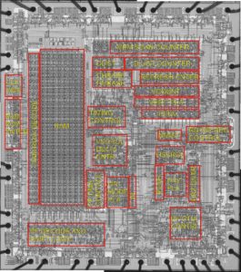
PIC12C5XX memory is organized into program memory and data memory. For devICes with more than 512 bytes of program memory, a paging scheme is used.
Program memory pages are accessed using one STATUS register bit. For the PIC12C509, PIC12C509A, PICCR509A and PIC12CE519 with a data memory register file of more than 32 registers, a banking scheme is used. Data memory banks are accessed using the File Select Register (FSR) when break mcu pic10f200 memory.
The PIC12C5XX devICes have a 12-bit Program Counter (PC) capable of addressing a 2K x 12 program memory space. Only the first 512 x 12 (0000h-01FFh) for the PIC12C508, PIC12C508A and PIC12CE518 and 1K x 12 (0000h-03FFh) for the PIC12C509, PIC12C509A, PIC12CR509A, and PIC12CE519 are physICally implemented.
Refer to Figure 4-1. Accessing a location above these boundaries will cause a wrap around within the first 512 x 12 space (PIC12C508, PIC12C508A and PIC12CE518) or 1K x 12 space (PIC12C509, PIC12C509A, PIC12CR509A and PIC12CE519). The effective reset vector is at 000h, (see Figure 4-1). Location 01FFh (PIC12C508, PIC12C508A and PIC12CE518) or location 03FFh (PIC12C509, PIC12C509A, PIC12CR509A and PIC12CE519) contains the internal clock oscillator calibration value. This value should never be overwritten when break microcontroller pic16f886 software memory.
As a program instruction is executed, the Program Counter (PC) will contain the address of the next program instruction to be executed. The PC value is increased by one every instruction cycle, unless an instruction changes the PC.
For a GOTO instruction, bits 8:0 of the PC are provided by the GOTO instruction word. The PC Latch (PCL) is mapped to PC<7:0>. Bit 5 of the STATUS register provides page information to bit 9 of the PC (Figure 4- 8).For a CALL instruction, or any instruction where the PCL is the destination before Copy IC, bits 7:0 of the PC again are provided by the instruction word. However, PC<8> does not come from the instruction word, but is always cleared (Figure 4-8).
Instructions where the PCL is the destination, or Modify PCL instructions, include MOVWF PC, ADDWF PC, and BSF PC,5. The Program Counter is set upon a RESET, whICh means that the PC addresses the last location in the last page i.e., the oscillator calibration instruction. After executing MOVLW XX, the PC will roll over to location 00h, and begin executing user code.
The STATUS register page preselect bits are cleared upon a RESET, whICh means that page 0 is pre-selected. Therefore, upon a RESET, a GOTO instruction will automatICally cause the program to jump to page 0 until the value of the page bits is altered if break IC.
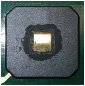
Copy Protected Chip PIC16C56 Code
Copy Protected Chip PIC16C56 Code include program of flash and data of eeprom memory, the embedded source code of microcontroller pic16c56 will be replicated after readout frm mcu pic16c56 memory;
The PIC12C5XX device contains an 8-bit ALU and working register. The ALU is a general purpose arithmetic unit. It performs arithmetic and Boolean functions between data in the working register and any register file when attack mcu attiny2313 memory for its firmware.
The ALU is 8-bits wide and capable of addition, subtraction, shift and logical operations. Unless otherwise mentioned, arithmetic operations are two’s complement in nature.
In two-operand instructions, typically one operand is the W (working) register. The other operand is either a file register or an immediate constant before Copy avr mcu atmega165a memory.
In single operand instructions, the operand is either the W register or a file register. The W register is an 8-bit working register used for ALU operations.
It is not an addressable register. Depending on the instruction executed, the ALU may affect the values of the Carry (C), Digit Carry (DC), and Zero (Z) bits in the STATUS register.
The C and DC bits operate as a borrow and digit borrow out bit, respectively, in subtraction. See theSUBWF andADDWF instructions for examples if copy mcu atmega162 flash memory.
A simplified block diagram is shown in Figure 3-1, with the corresponding device pins described in Table 3-1. The PIC12C5XX can directly or indirectly address its register files and data memory.
All special function registers including the code counter are mapped in the data memory. The PIC12C5XX has a highly orthogonal (symmetrical) instruction set that makes it possible to carry out any operation on any register using any addressing mode. This symmetrical nature and lack of ‘special optimal situations’ make codeming with the PIC12C5XX simple yet efficient. In addition, the learning curve is reduced significantly.
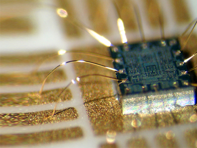
Extract Chip PIC12LF510 Code
Extract Chip PIC12LF510 code from embedded flash memory, the firmware conside inside locked mcu pic12lf510 will be readout after crack microcontroller;
The PICkit™ 2 Development Programmer is a low-cost programmer with an easy-to-use interface for programming many of Microchip ’s baseline, mid-range and PIC18F families of Flash memory.
The PICkit 2 Starter Kit includes a prototyping development board, twelve sequential lessons, software and HI-TECH’s PICC™ Lite C compiler, and is designed to help get up to speed quickly using PIC® break mcu pic16f631 flash memory.
The kit provides everything needed to program, evaluate and develop applications using Microchip ’s powerful, mid-range Flash memory family.
A wide variety of demonstration, development and evaluation boards for various PIC MCUs and dsPIC DSCs allows quick application development on fully functional systems if break microcontroller pic16f628a.
Most boards include prototyping areas for adding custom circuitry and provide application firmware and source code for examination and modification after Extract Chip code.
The boards support a variety of features, including LEDs, temperature sensors, switches, speakers, RS-232 interfaces, LCD displays, potentiometers and additional EEPROM memory.
The demonstration and development boards can be used in teaching environments, for prototyping custom circuits and for learning about various Chip applications after Extract attack mcu pic16f711 hex.
In addition to the PICDEM™ and dsPICDEM™ demonstration/development board series of circuits, Microchip has a line of evaluation kits and demonstration software for analog filter design, KEELOQ® security ICs, CAN, IrDA®, PowerSmart® battery management, SEEVAL® evaluation system, Sigma-Delta ADC, flow rate sensing, plus many more.
Check the Microchip web page (www.microchip .com) and the latest “Product Selector Guide” (DS00148) for the complete list of demonstration, development and evaluation kits.
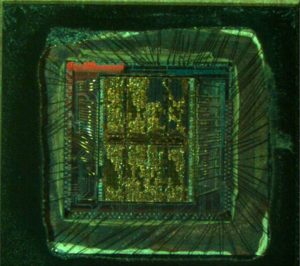
Copy Chip ST10F168SQ6 Software
Copy Chip ST10F168SQ6 Software from its encrypted flash and eeprom memory, extract MCU firmware and make microcontroller st10f168sq6 cloning units;
HIGH PERFORMANCE CPU
– 16-BIT CPU WITH 4-STAGE PIPELINE
– 80ns INSTRUCTION CYCLE TIME AT 25MHz CPU CLOCK
– 400ns 16 X 16-BIT MULTIPLICATION
– 800ns 32 / 16-BIT DIVISION
– ENHANCED BOOLEAN BIT MANIPULATION FACILITIES
– ADDITIONAL INSTRUCTIONS TO SUPPORT HLL AND OPERATING SYSTEMS
– SINGLE-CYCLE CONTEXT SWITCHING SUP-
PQFP144 (28 x 28 mm) (Plastic Quad Flat Pack)
PORT A/D CONVERTER
MEMORY ORGANIZATION
– 256K BYTE ON-CHIP FLASH MEMORY
– 10K ERASING / PROGRAMMING CYCLES
– UP TO 16M BYTE LINEAR ADDRESS SPACE
FOR CODE AND DATA (5M BYTE WITH CAN) when break microcontroller s3f9454 software
– 2K BYTE ON-CHIP INTERNAL RAM (IRAM)
– 6K BYTE ON-CHIP EXTENSION RAM (XRAM)
– 20 YEAR DATA RETENTIO N TIME
FAST AND FLEXIBLE BUS
– PROGRAMMABLE EXTERNAL BUS CHARAC-
TE- RISTICS FOR DIFFERENT ADDRESS RANGES
– 8-BIT OR 16-BIT EXTERNAL DATA BUS
– MULTIPLEXED OR DEMULTIPLEXED EXTER-NAL ADDRESS / DATA BUSES
– FIVE PROGRAMMABLE CHIP-SELECT SIGNALS
– HOLD-ACKNOWLEDGE BUS ARBITRATION SUPPORT INTERRUPT
– 16-CHANNEL 10-BIT after read microchip mcu pic32mx440f512h bin
– 7.76µS CONVERSION TIME
FAIL-SAFE PROTECTIO N
– PROGRAMMABLE WATCHDOG TIMER
– OSCILLATOR WATCHDOG
ON-CHIP CAN 2.0B INTERFACE
ON-CHIP BOOTSTR AP LOADER
CLOCK GENERATION
– ON-CHIP PLL
– DIRECT OR PRESCALED CLOCK INPUT.
UP TO 111 GENERAL PURPOSE I/O LINES
– INDIVIDUALLY PROGRAMMABLE AS INPUT,
OUTPUT OR SPECIAL FUNCTION.
– PROGRAMMABLE THRESHOLD (HYSTERESIS)
IDLE AND POWER DOWN MODES
SINGLE VOLTAGE SUPPLY: 5V ±10%
144-PIN PQFP PACKAGE
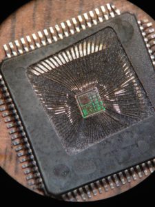
Reverse Engineering IC PIC18F248 Binary
Reverse Engineering IC PIC18F248 and locate the fuse bit position, crack mcu pic18f248 flash memory by focus ion beam and copy the embedded firmware from microcontroller pic18f248;
High-Performance RISC CPU:
· Linear program memory addressing up to 2 Mbytes
· Linear data memory addressing to 4 Kbytes
· Up to 10 MIPS operation
· DC – 40 MHz clock input
· 4 MHz-10 MHz oscillator/clock input with PLL active when copy microcontroller pic16f737 flash memory
· 16-bit wide instructions, 8-bit wide data path
· Priority levels for interrupts
· 8 x 8 Single-Cycle Hardware Multiplier
Peripheral Features:
· High current sink/source 25 mA/25 mA
· Three external interrupt pins
· Timer0 module: 8-bit/16-bit timer/counter with 8-bit programmable prescaler
· Timer1 module: 16-bit timer/counter
· Timer2 module: 8-bit timer/counter with 8-bit period register (time base for PWM)
· Timer3 module: 16-bit timer/counter
· Secondary oscillator clock option – Timer1/Timer3
· Capture/Compare/PWM (CCP) modules; CCP pins can be configured as:
– Capture input: 16-bit, max resolution 6.25 ns
– Compare: 16-bit, max resolution 100 ns (TCY) before break mcu pic18f442 software
– PWM output: PWM resolution is 1 to 10-bit Max. PWM freq. @:8-bit resolution = 156 kHz 10-bit resolution = 39 kHz
· Enhanced CCP module which has all the features of the standard CCP module, but also has the following features for advanced motor control:
– 1, 2 or 4 PWM outputs
– Selectable PWM polarity
– Programmable PWM dead time
· Master Synchronous Serial Port (MSSP) with two modes of operation:
– 3-wire SPI™ (Supports all 4 SPI modes) after Reverse engineering IC
– I2C™ Master and Slave mode
· Addressable USART module:
– Supports interrupt-on-address bit
Advanced Analog Features:
· 10-bit, up to 8-channel Analog-to-Digital Converter module (A/D) with:
– Conversion available during Sleep
– Up to 8 channels available
· Analog Comparator module:
– Programmable input and output multiplexing
· Comparator Voltage Reference module
· Programmable Low-Voltage Detection (LVD) module:
– Supports interrupt-on-Low-Voltage Detection
· Programmable Brown-out Reset (BOR)
CAN bus Module Features:
· Complies with ISO CAN Conformance Test
· Message bit rates up to 1 Mbps
· Conforms to CAN 2.0B Active Spec with:
– 29-bit Identifier Fields
– 8-byte message length
– 3 Transmit Message Buffers with prioritization
– 2 Receive Message Buffers
– 6 full, 29-bit Acceptance Filters
– Prioritization of Acceptance Filters
– Multiple Receive Buffers for High Priority Messages to prevent loss due to overflow
– Advanced Error Management Features
Special Microcontroller Features:
· Power-on Reset (POR), Power-up Timer (PWRT) and Oscillator Start-up Timer (OST)
· Watchdog Timer (WDT) with its own on-chip RC oscillator
· Programmable code protection
· Power-saving Sleep mode
· Selectable oscillator options, including:
– 4x Phase Lock Loop (PLL) of primary oscillator
– Secondary Oscillator (32 kHz) clock input
· In-Circuit Serial ProgrammingTM (ICSPTM) via two pins IC Flash Technology:
· Low-power, high-speed Enhanced Flash technology
· Fully static design Wide operating voltage range (2.0V to 5.5V) Industrial and Extended temperature ranges
Break IC PIC18F242 Software
Break IC PIC18F242 Software is a process to unlock encrypted mcu pic18f242 protection and open locked microcontroller pic18f242 flash memory silicon package;
Break IC PIC18F242 Software is a process to unlock encrypted mcu pic18f242 protection and open locked microcontroller pic18f242 flash memory silicon package
High Performance RISC CPU:
· C compiler optimized architecture/instruction set
– Source code compatible with the PIC16 and PIC17 instruction sets
· Linear program memory addressing to 32 Kbytes
· Linear data memory addressing to 1.5 Kbytes
· Up to 10 MIPs operation:
– DC – 40 MHz osc./clock input
– 4 MHz – 10 MHz osc./clock input with PLL active
· 16-bit wide instructions, 8-bit wide data path
· Priority levels for interrupts
· 8 x 8 Single Cycle Hardware Multiplier
Peripheral Features:
· High current sink/source 25 mA/25 mA
· Three external interrupt pins
· Timer0 module: 8-bit/16-bit timer/counter with 8-bit programmable prescaler
· Timer1 module: 16-bit timer/counter
· Timer2 module: 8-bit timer/counter with 8-bit period register (time-base for PWM)
· Timer3 module: 16-bit timer/counter
· Secondary oscillator clock option – Timer1/Timer3
· Two Capture/Compare/PWM (CCP) modules. CCP pins that can be configured as:
– Capture input: capture is 16-bit, max. resolution 6.25 ns (TCY/16)
– Compare is 16-bit, max. resolution 100 ns (TCY)
– PWM output: PWM resolution is 1- to 10-bit, max. PWM freq. @: 8-bit resolution = 156 kHz 10-bit resolution = 39 kHz
· Master Synchronous Serial Port (MSSP) module,
Two modes of operation:
– 3-wire SPI™ (supports all 4 SPI modes)
– I2C™ Master and Slave mode
Peripheral Features (Continued):
· Addressable USART module:
– Supports RS-485 and RS-232
· Parallel Slave Port (PSP) module
Analog Features:
· Compatible 10-bit Analog-to-Digital Converter module (A/D):
– Fast sampling rate
– Conversion available during SLEEP
– Linearity ≤ 1 LSb
· Programmable Low Voltage Detection (PLVD)
– Supports interrupt on-Low Voltage Detection
· Programmable Brown-out Reset (BOR)
Reverse Engineering Microcontroller PIC16HV610 Program
Reverse Engineering Microcontroller PIC16HV610 is a process to locate the fuse bit of mcu and unlock pic16hv610 protection, extract mcu code from pic16hv610 memory;
Reverse Engineering Microcontroller PIC16HV610 Program
We can Reverse engineering Microcontroller PIC16HV610 Program, please view the Microcontroller PIC16HV610 features for your reference:
High-Performance RISC CPU:
· Only 35 instructions to learn:
– All single-cycle instructions except branches
· Operating speed:
– DC – 20 MHz oscillator/clock input
– DC – 200 ns instruction cycle
· Interrupt capability
· 8-level deep hardware stack
· Direct, Indirect and Relative Addressing modes
Special Microcontroller Features:
· Precision Internal Oscillator:
– Factory calibrated to ±1%, typical
– User selectable frequency: 4 MHz or 8 MHz
· Power-Saving Sleep mode
· Voltage range:
– PIC16F610/616: 2.0V to 5.5V
– PIC16HV610/616: 2.0V to user defined maximum (see note)
· Industrial and Extended Temperature range
· Power-on Reset (POR)
· Power-up Timer (PWRT) and Oscillator Start-up Timer (OST)
· Brown-out Reset (BOR)
· Watchdog Timer (WDT) with independent oscillator for reliable operation before Reverse engineering Microcontroller
· Multiplexed Master Clear with pull-up/input pin
· Programmable code protection
· High Endurance Flash:
– 100,000 write Flash endurance
– Flash retention: > 40 years
Low-Power Features:
· Standby Current:
– 50 nA @ 2.0V, typical
· Operating Current:
– 20 ìA @ 32 kHz, 2.0V, typical
– 220 ìA @ 4 MHz, 2.0V, typical
· Watchdog Timer Current:
– 1 ìA @ 2.0V, typical
Peripheral Features:
· Shunt Voltage Regulator (PIC16HV610/616 only):
– 5 volt regulation
– 4 mA to 50 mA shunt range
· 11 I/O pins and 1 input only
– High current source/sink for direct LED drive
– Interrupt-on-Change pins
– Individually programmable weak pull-ups
· Analog Comparator module with:
– Two analog comparators
– Programmable on-chip voltage reference (CVREF) module (% of VDD)
– Fixed Voltage Reference
– Comparator inputs and outputs externally accessible
– SR Latch
– Built-In Hysteresis (user selectable)
· Timer0: 8-bit timer/counter with 8-bit programmable prescaler
· Enhanced Timer1:
– 16-bit timer/counter with prescaler
– External Timer1 Gate (count enable)
– Option to use OSC1 and OSC2 in LP mode as Timer1 oscillator if INTOSC mode selected
– Timer1 oscillator
· In-Circuit Serial ProgrammingTM (ICSPTM) via two pins
PIC16F616/16HV616 only:
· A/D Converter:
– 10-bit resolution
– 8 external input channels
– 2 internal reference channels
· Timer2: 8-bit timer/counter with 8-bit period register, prescaler and postscaler
· Enhanced Capture, Compare, PWM module:
– 16-bit Capture, max. resolution 12.5 ns
– 16-bit Compare, max. resolution 200 ns
– 10-bit PWM with 1, 2 or 4 output channels, programmable “dead time”, max. frequency 20 kHz
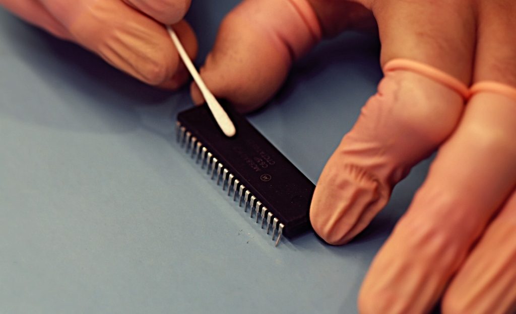
Recovery Microcontroller PIC16F877 Program
Recovery Microcontroller PIC16F877 Program from embedded flash and eeprom memory, the firmware of locked mcu pic16f877 will be cloned after extract microchip pic16f877 code.
PORTC is an 8-bit wide, bi-directional port. The corresponding data direction register is TRISC. Setting a TRISC bit (= 1) will make the corresponding PORTC pin an input (i.e., put the corresponding output driver in a Hi-Impedance mode). Clearing a TRISC bit (= 0) will make the corresponding PORTC pin an output (i.e., put the contents of the output latch on the selected pin).
PORTC is multiplexed with several peripheral functions When the I2C module is enabled, the PORTC<4:3> pins can be configured with normal I2C levels, or with SMBus levels by using the CKE bit (SSPSTAT<6>).
When enabling peripheral functions, care should be taken in defining TRIS bits for each PORTC pin. Some peripherals override the TRIS bit to make a pin an output, while other peripherals override the TRIS bit to make a pin an input if extract avr ic Microcontroller.
Since the TRIS bit override is in effect while the peripheral is enabled, recovery-modify-write instructions (BSF, BCF, XORWF) with TRISC as destination, should be avoided. The user should refer to the corresponding peripheral section for the correct TRIS bit settings.
PORTE and TRISE are not implemented on the PORTE has three pins (RE0/RD/AN5, RE1/WR/AN6, and RE2/CS/AN7) which are individually configureable as inputs or outputs. These pins have Schmitt Trigger input buffers after extract pld chip flash memory.
The PORTE pins become the I/O control inputs for the microprocessor port when bit PSPMODE (TRISE<4>) is set. In this mode, the user must make certain that the TRISE<2:0> bits are set, and that the pins are configured as digital inputs. Also ensure that ADCON1 is configured for digital I/O. In this mode, the input buffers are TTL.
Register 3-1 shows the TRISE register, which also controls the parallel slave port operation. PORTE pins are multiplexed with analog inputs. When selected for analog input, these pins will recovery as ’0’s. TRISE controls the direction of the RE pins, even when they are being used as analog inputs. The user must make sure to keep the pins configured as inputs when using them as analog inputs.
The Parallel Slave Port (PSP) is not implemented on the PIC16F873 or PIC16F876. PORTD operates as an 8-bit wide Parallel Slave Port or microprocessor port, when control bit PSPMODE (TRISE<4>) is set. In Slave mode, it is asynchronously recoveryable and writable by the external world through RD control input pin RE0/RD and WR control input pin RE1/WR.
The PSP can directly interface to an 8-bit microprocessor data bus. The external microprocessor can recovery or write the PORTD latch as an 8-bit latch. Setting bit PSPMODE enables port pin RE0/RD to be the RD input, RE1/WR to be the WR input and RE2/CS to be the CS (microcontroller select) input. For this functionality, the corresponding data direction bits of the TRISE register (TRISE<2:0>) must be configured as inputs (set).
The A/D port configuration bits PCFG3:PCFG0 (ADCON1<3:0>) must be set to configure pins RE2:RE0 as digital I/O. There are actually two 8-bit latches: one for data output, and one for data input. The user writes 8-bit data to the PORTD data latch and recoverys data from the port pin latch (note that they have the same address).
In this mode, the TRISD register is ignored, since the external device is controlling the direction of data flow. A write to the PSP occurs when both the CS and WR lines are first detected low. When either the CS or WR lines become high (level triggered), the Input Buffer Full (IBF) status flag bit (TRISE<7>) is set on the Q4 clock cycle, following the next Q2 cycle, to signal the write is complete (Figure 3-10).
The interrupt flag bit PSPIF (PIR1<7>) is also set on the same Q4 clock cycle. IBF can only be cleared by recoverying the PORTD input latch. The Input Buffer Overflow (IBOV) status flag bit (TRISE<5>) is set if a second write to the PSP is attempted when the previous byte has not been recovery out of the buffer.