Archive for the ‘Reverse Engineer Microcontroller’ Category
 Copy Microcontroller PIC16F747 Code
Copy Microcontroller PIC16F747 Code from embedded flash and eeprom memory, and extract the firmware from MCU pic16f747 memory after crack MCU protection;
Copy Microcontroller PIC16F747 Code from embedded flash and eeprom memory, and extract the firmware from MCU pic16f747 memory after crack MCU protection
Special Microcontroller Features:
· Fail-Safe Clock Monitor for protecting critical applications against crystal failure;
· Two-Speed Start-up mode for immediate code execution
· Power-on Reset (POR), Power-up Timer (PWRT) and Oscillator Start-up Timer (OST)
· Programmable Code Protection
· Processor Read Access to Program Memory
· Power-Saving Sleep mode
· In-Circuit Serial Programming (ICSP) via two pins
· MPLAB® In-Circuit Debug (ICD) via two pins
· MCLR pin function replaceable with input only pin if Copy chip pic16f870 program
DEVICE OVERVIEW
This document contains device specific information about the following devices:
PIC16F737/767 devices are available only in 28-pin packages, while PIC16F747/777 devices are available in 40-pin and 44-pin packages. All devices in the PIC16F7X7 family share common architecture with the following differences:
· The PIC16F737 and PIC16F767 have one-half of the total on-chip memory of the PIC16F747 and PIC16F777.
· The 28-pin devices have 3 I/O ports, while the 40/44-pin devices have 5.
· The 28-pin devices have 16 interrupts, while the 40/44-pin devices have 17.
· The 28-pin devices have 11 A/D input channels, while the 40/44-pin devices have 14.
· The Parallel Slave Port is implemented only on the 40/44-pin devices.
· Low-Power modes: RC_RUN allows the core and peripherals to be clocked from the INTRC, while SEC_RUN allows the core and peripherals to be clocked from the low-power Timer1. Refer to
Section 4.7 “Power-Managed Modes” for further details for the purpose of break pic18f8722 Microcontroller code.
· Internal RC oscillator with eight selectable frequencies, including 31.25 kHz, 125 kHz, 250 kHz, 500 kHz, 1 MHz, 2 MHz, 4 MHz and 8 MHz. The INTRC can be configured as a primary or secondary clock source. Refer to Section 4.5 “Internal Oscillator Block” for further details.
Copy Microcontroller PIC16F639 Heximal
Copy Microcontroller PIC16F639 Heximal needs to extract the flash program from microprocessor PIC16F639 and then crack microcontroller pic16f639 security fuse bit;
A single comparator is shown in Figure 6-1, along with the relationship between the analog input levels and the digital output. When the analog input at VIN+ is less than the analog input VIN-, the output of the comparator is a digital low level. When the analog input at VIN+ is greater than the analog input VIN-, the output of the comparator is a digital high level. The shaded areas of the output of the comparator in Figure 6-1 represent the uncertainty due to input offsets and response time.
The polarity of the comparator output can be inverted by setting the CINV bit (CMCON<4>). Clearing CINV results in a non-inverted output. A complete table showing the output state versus input conditions and VIN-the polarity bit.
There are eight modes of operation for the comparator. The CMCON register, shown in Register 6-1, is used to select the mode. Figure 6-2 shows the eight possible modes. The TRISA register controls the data direction of the comparator pins for each mode.
If the Comparator mode is changed, the comparator output
The CMCON register, shown in Register 6-1, is used to select the mode. Figure 6-2 shows the eight possible modes. The TRISA register controls the data direction of the comparator pins for each mode.
A simplified circuit for an analog input is shown in Figure 6-3. Since the analog pins are connected to a digital output, they have reverse biased diodes to VDD and VSS. The analog input, therefore, must be between VSS and VDD. If the input voltage deviates from this libri the polarity bit.
Response time is the minimum time, after selecting a new reference voltage or input source, before the comparator output is ensured to have a valid level. If the internal reference is changed, the maximum delay of the internal voltage reference must be considered when using the comparator outputs. Otherwise, the maximum delay of the comparators should be used H-CN;
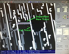
Recover MCU ATmega2561V Eeprom
Recover MCU ATmega2561V Eeprom content needs to crack mcu atmega2561v protective system by focus ion beam and then copy the firmware inside flash and eeprom memory of microcontroller atmega2561v to new ones for same functionality;
This documentation contains simple code examples that briefly show how to use various parts of the device. Be aware that not all C compiler vendors include bit definitions in the header files and interrupt handling in C is compiler dependent. Please confirm with the C compiler documentation for more details.
These code examples assume that the part specific header file is included before compilation. For I/O registers located in extended I/O map, “IN”, “OUT”, “SBIS”, “SBIC”, “CBI”, and “SBI” instructions must be replaced with instructions that allow access to extended I/O. Typically “LDS” and “STS” combined with “SBRS”, “SBRC”, “SBR”, and “CBR” if Recover atmega2560 MCU flash.
This section discusses the AVR core architecture in general. The main function of the CPU core is to ensure correct program execution. The CPU must therefore be able to access memories, perform calculations, control peripherals, and handle interrupts.
In order to maximize performance and parallelism, the AVR uses a Harvard architecture – with separate memories and buses for program and data. Instructions in the program memory are executed with a single level pipelining. While one instruction is being executed, the next instruction is pre-fetched from the program memory.
This concept enables instructions to be executed in every clock cycle. The program memory is In-System Reprogrammable Flash memory. The fast-access Register File contains 32 x 8-bit general purpose working registers with a single clock cycle access time.
This allows single-cycle Arithmetic Logic Unit (ALU) operation. In a typical ALU operation, two operands are output from the Register File, the operation is executed, and the result is stored back in the Register File – in one clock cycle if Reverse engineering atmega1281 MCU.
Six of the 32 registers can be used as three 16-bit indirect address register pointers for
Data Space addressing – enabling efficient address calculations. One of the these address pointers can also be used as an address pointer for look up tables in Flash program memory. These added function registers are the 16-bit X-, Y-, and Z-register, described later in this section.
The ALU supports arithmetic and logic operations between registers or between a constant and a register. Single register operations can also be executed in the ALU. After an arithmetic operation, the Status Register is updated to reflect information about the result of the operation.
Program flow is provided by conditional and unconditional jump and call instructions, able to directly address the whole address space. Most AVR instructions have a single 16-bit word format. Every program memory address contains a 16- or 32-bit instruction.
Program Flash memory space is divided in two sections, the Boot Program section and the Application Program section. Both sections have dedicated Lock bits for write and read/write protection. The SPM instruction that writes into the Application Flash memory section must reside in the Boot Program section.
Reverse Engineering Microcontroller ATMEGA1281 Program
Reverse Engineering Microcontroller ATMEGA1281 purpose is to unlock mcu atmega1281 flash memory and then copy Program and data from atmega1281 memory to new MCU;
Features
High Performance, Low Power AVR® 8-Bit Microcontroller
Advanced RISC Architecture
– 135 Powerful Instructions – Most Single Clock Cycle Execution
– 32 x 8 General Purpose Working Registers
– Fully Static Operation
– Up to 16 MIPS Throughput at 16 MHz
– On-Chip 2-cycle Multiplier
Non-volatile Program and Data Memories
– 64K/128K/256K Bytes of In-System Self-Programmable Flash
Endurance: 10,000 Write/Erase Cycles
– Optional Boot Code Section with Independent Lock Bits
In-System Programming by On-chip Boot Program
True Read-While-Write Operation
– 4K Bytes EEPROM
Endurance: 100,000 Write/Erase Cycles
– 8K Bytes Internal SRAM
– Up to 64K Bytes Optional External Memory Space
– Programming Lock for Software Security
JTAG (IEEE std. 1149.1 compliant) Interface
– Boundary-scan Capabilities According to the JTAG Standard
– Extensive On-chip Debug Support when copy cpld epm9320arc208
– Programming of Flash, EEPROM, Fuses, and Lock Bits through the JTAG Interface
Peripheral Features
– Two 8-bit Timer/Counters with Separate Prescaler and Compare Mode
– Four 16-bit Timer/Counter with Separate Prescaler, Compare- and Capture Mode
– Real Time Counter with Separate Oscillator
– Four 8-bit PWM Channels
– Six/Twelve PWM Channels with Programmable Resolution from 2 to 16 Bits (ATmega1281/2561, ATmega640/1280/2560)
– Output Compare Modulator
– 8/16-channel, 10-bit ADC
– Two/Four Programmable Serial USART (ATmega1281/2561,ATmega640/1280/2560)
– Master/Slave SPI Serial Interface
– Byte Oriented 2-wire Serial Interface
– Programmable Watchdog Timer with Separate On-chip Oscillator after Reverse engineering Microcontroller
– On-chip Analog Comparator
– Interrupt and Wake-up on Pin Change
Special Microcontroller Features
– Power-on Reset and Programmable Brown-out Detection
– Internal Calibrated Oscillator
– External and Internal Interrupt Sources when Reverse engineering Microcontroller
– Six Sleep Modes: Idle, ADC Noise Reduction, Power-save, Power-down, Standby, and Extended Standby
I/O and Packages
– 51/86 Programmable I/O Lines (ATmega1281/2561, ATmega640/1280/2560)
– 64-lead (ATmega1281/2561)
– 100-lead (ATmega640/1280/2560)
– 100-lead TQFP (64-lead TQFP Option)
Temperature Range:
– -40°C to 85°C Industrial if Reverse engineering Microcontroller
Speed Grade:
Programmable Flash
– ATmega1281/2561V/ATmega640/1280/2560V: 0 – 4 MHz @ 1.8 – 5.5V, 0 – 8 MHz @ 2.7 – 5.5V
– ATmega640/1280/1281/2560/2561: 0 – 8 MHz @ 2.7 – 5.5V, 0 – 16 MHz @ 4.5 – 5.5V before Reverse engineering Microcontroller
Copy Microcontroller PIC16F882 Heximal
Copy Microcontroller PIC16F882 Heximal from flash memory and eeprom memory, unlock mcu pic16f882 protection and crack microcontroller pic16f882 security fuse bit to unleash embedded firmware.
High-Performance RISC CPU:
· Only 35 Instructions to Learn:
– All single-cycle instructions except branches
· Operating Speed:
– DC – 20 MHz oscillator/clock input
– DC – 200 ns instruction cycle
· Interrupt Capability
· 8-Level Deep Hardware Stack
· Direct, Indirect and Relative Addressing modes
Special Microcontroller Features:
· Precision Internal Oscillator:
– Factory calibrated to ±1%
– Software selectable frequency range of 8 MHz to 31 kHz
– Software tunable
– Two-Speed Start-up mode
– Crystal fail detect for critical applications
– Clock mode switching during operation for power savings
· Power-Saving Sleep mode
· Wide Operating Voltage Range (2.0V-5.5V)
· Industrial and Extended Temperature Range
· Power-on Reset (POR)
· Power-up Timer (PWRT) and Oscillator Start-up Timer (OST)
· Brown-out Reset (BOR) with Software Control Option
· Enhanced Low-Current Watchdog Timer (WDT) with On-Chip Oscillator (software selectable nominal 268 seconds with full prescaler) with software enable
· Multiplexed Master Clear with Pull-up/Input Pin
· Programmable Code Protection
· High Endurance Flash/EEPROM Cell:
– 100,000 write Flash endurance
– 1,000,000 write EEPROM endurance
– Flash/Data EEPROM retention: > 40 years
· Program Memory Read/Write during run time
· In-Circuit Debugger (on board)
Reverse Engineering Microcontroller ATMEGA2560V Firmware
We can Reverse engineering Microcontroller ATMEGA2560V Firmware, please view the Microcontroller ATMEGA2560V features for your reference:
The ATmega2560v implements 256 bytes of RAM. The upper 128 bytes of RAM occupy a parallel space to the Special Function Registers. That means the upper 128 bytes have the same addresses as the SFR space but are physically separate from SFR space.
When an instruction accesses an internal location above address 7FH, the address mode used in the instruction specifies whether the CPU accesses the upper 128 bytes of RAM or the SFR space. Instructions that use direct addressing access SFR space.
For example, the following direct addressing instruction accesses the SFR at location 0A0H (which is P2). MOV 0A0H, #data
Instructions that use indirect addressing access the upper 128 bytes of RAM. For example, the following indirect addressing instruction, where R0 contains 0A0H, accesses the data byte at address 0A0H, rather than P2 (whose address is 0A0H) before Reverse Engineering Microcontroller ATMEGA2560V Firmware.
Note that stack operations are examples of indirect addressing, so the upper 128 bytes of data RAM are available as stack, The programmable Watchdog Timer (WDT) operates from an independent oscillator. The prescaler bits, PS0, PS1 and PS2 in SFR WCON are used to set the period of the Watchdog Timer from 16 ms to 2048 ms.
The available timer periods are shown in the following table and the actual timer periods (at VCC = 5V) are within ±30% of the nominal. The WDT is disabled by Power-on Reset and during Power Down. It is enabled by setting the WDTEN bit in SFR WCON (address = 96H) after Reverse Engineering Microcontroller ATMEGA2560V Firmware.
The WDT is reset by setting the WDTRST bit in WCON. When the WDT times out without being reset or disabled, an internal RST pulse is generated to reset the CPU. Table 7. Watchdog Timer Period Selection space.
Timer 0 and Timer 1 in the AT89LS53 operate the same way as Timer 0 and Timer 1 in the AT89C51, AT89C52 and AT89C55. For further information, see the October 1995 Microcontroller Data Book, page 2-45, section titled, “Timer/Counters.”
Timer 2 is a 16 bit Timer/Counter that can operate as either a timer or an event counter. The type of operation is selected by bit C/T2 in the SFR T2CON (shown in Table 2). Timer 2 has three operating modes: capture, auto-reload (up or down counting), and baud rate generator before Reverse Engineering Microcontroller ATMEGA2560V Firmware.
The modes are selected by bits in T2CON, as shown in Table 8. Timer 2 consists of two 8-bit registers, TH2 and TL2. In the Timer function, the TL2 register is incremented every machine cycle. Since a machine cycle consists of 12 oscillator periods, the count rate is 1/12 of the oscillator frequency.
In the Counter function, the register is incremented in response to a 1-to-0 transition at its corresponding external input pin, T2. In this function, the external input is sampled during S5P2 of every machine cycle. When the samples show a high in one cycle and a low in the next cycle, the count is incremented.
The new count value appears in the register during S3P1 of the cycle following the one in which the transition was detected. Since two machine cycles (24 oscillator periods) are required to recognize a 1-to-0 transition, the maximum count rate is 1/24 of the oscillator frequency. To ensure that a given level is sampled at least once before it changes, the level should be held for at least one full machine cycle when Reverse Engineering Microcontroller ATMEGA2560V Firmware.
Reverse Engineering Microcontroller ATmega640
Reverse Engineering Microcontroller ATmega640 and readout the embedded content from mcu atmega640, atmega640 mcu protection can be unlocked by focus ion beam;
Features
High Performance, Low Power AVR® 8-Bit Microcontroller
Advanced RISC Architecture
– 135 Powerful Instructions – Most Single Clock Cycle Execution when copy pic18f252 Microcontroller
– 32 x 8 General Purpose Working Registers
– Fully Static Operation
– Up to 16 MIPS Throughput at 16 MHz
– On-Chip 2-cycle Multiplier
High Endurance Non-volatile Memory Segments
– 64K/128K/256K Bytes of In-System Self-Programmable Flash
– 4K Bytes EEPROM
– 8K Bytes Internal SRAM
– Write/Erase Cycles:10,000 Flash/100,000 EEPROM
– Data retention: 20 years at 85°C/ 100 years at 25°C
– Optional Boot Code Section with Independent Lock Bits after recover dspic30f6013a Microcontroller
In-System Programming by On-chip Boot Program
True Reverse engineering-While-Write Operation
– Programming Lock for Software Security
Endurance: Up to 64K Bytes Optional External Memory Space
JTAG (IEEE std. 1149.1 compliant) Interface
– Boundary-scan Capabilities According to the JTAG Standard
– Extensive On-chip Debug Support
– Programming of Flash, EEPROM, Fuses, and Lock Bits through the JTAG Interface
Peripheral Features
– Two 8-bit Timer/Counters with Separate Prescaler and Compare Mode
– Four 16-bit Timer/Counter with Separate Prescaler, Compare- and Capture Mode
– Real Time Counter with Separate Oscillator
– Four 8-bit PWM Channels
– Six/Twelve PWM Channels with Programmable Resolution from 2 to 16 Bits
(ATmega1281/2561, ATmega640/1280/2560)
– Output Compare Modulator
– 8/16-channel, 10-bit ADC (ATmega1281/2561, ATmega640/1280/2560) after Reverse engineering Microcontroller
– Two/Four Programmable Serial USART (ATmega1281/2561,ATmega640/1280/2560)
– Master/Slave SPI Serial Interface
– Byte Oriented 2-wire Serial Interface
– Programmable Watchdog Timer with Separate On-chip Oscillator
– On-chip Analog Comparator
– Interrupt and Wake-up on Pin Change
Special Microcontroller Features
– Power-on Reset and Programmable Brown-out Detection
– Internal Calibrated Oscillator
– External and Internal Interrupt Sources
– Six Sleep Modes: Idle, ADC Noise Reduction, Power-save, Power-down, Standby, and Extended Standby I/O and Packages
– 54/86 Programmable I/O Lines (ATmega1281/2561, ATmega640/1280/2560)
– 64-pad QFN/MLF, 64-lead TQFP (ATmega1281/2561)
– 100-lead TQFP, 100-ball CBGA (ATmega640/1280/2560)
– RoHS/Fully Green
Temperature Range:
– -40°C to 85°C Industrial
Ultra-Low Power Consumption
– Active Mode: 1 MHz, 1.8V: 500 µA
– Power-down Mode: 0.1 µA at 1.8V
Speed Grade:
– ATmega640V/ATmega1280V/ATmega1281V:
0 – 4 MHz @ 1.8 – 5.5V, 0 – 8 MHz @ 2.7 – 5.5V
– ATmega2560V/ATmega2561V:
0 – 2 MHz @ 1.8 – 5.5V, 0 – 8 MHz @ 2.7 – 5.5V
– ATmega640/ATmega1280/ATmega1281:
0 – 8 MHz @ 2.7 – 5.5V, 0 – 16 MHz @ 4.5 – 5.5V
– ATmega2560/ATmega2561:
0 – 16 MHz @ 4.5 – 5.5V
Recover MCU ATtiny861V Flash
Recover MCU ATtiny861V Flash program and eeprom data, crack microcontroller attiny861v protective system and read the firmware out from embedded processor attiny861v memory;
A map of the on-chip memory area called the Special Function Register (SFR) space is shown in Table 1.
Note that not all of the addresses are occupied, and unoccupied addresses may not be implemented on the chip. Recover accesses to these addresses will in general return random data, and write accesses will have an indeterminate effect if attack pic18lf4520 MCU.
User software should not write 1s to these unlisted locations, since they may be used in future products to invoke new features. In that case, the reset or inactive values of the new bits will always be 0.
Timer 2 Registers: Control and status bits are contained in registers T2CON (shown in Table 2) and T2MOD (shown in Table ) for Timer 2. The register pair (RCAP2H, RCAP2L) are the Capture/Reload registers for Timer 2 in 16-bit capture mode or 16-bit auto-reload mode.
Interrupt Registers: The individual interrupt enable bits are in the IE register. Two priorities can be set for each of the six interrupt sources in the IP register.
Table 2. T2CON – Timer/Counter 2 Control Register
MCS-51 devices have a separate address space for Program and Data Memory. Up to 64K bytes each of external Program and Data Memory can be addressed.
If the EA pin is connected to GND, all program fetches are directed to external memory. On the AT89LS52, if EA is connected to VCC, program fetches to addresses 0000H through 1FFFH are directed to internal memory and fetches to addresses 2000H through FFFFH are directed to external memory when copy pic18f458 MCU binary.
The AT89LS52 implements 256 bytes of on-chip RAM. The upper 128 bytes occupy a parallel address space to the Special Function Registers. This means that the upper 128 bytes have the same addresses as the SFR space but are physically separate from SFR space.
When an instruction accesses an internal location above address 7FH, the address mode used in the instruction specifies whether the CPU accesses the upper 128 bytes of RAM or the SFR space. Instructions which use direct addressing access of the SFR space.
For example, the following direct addressing instruction accesses the SFR at location 0A0H (which is P2). MOV 0A0H, #data Instructions that use indirect addressing access the upper 128 bytes of RAM. For example, the following indirect addressing instruction, where R0 contains 0A0H, accesses the data byte at address 0A0H, rather than P2 (whose address is 0A0H) after Recover MCU.
MOV @R0, #data Note that stack operations are examples of indirect addressing, so the upper 128 bytes of data RAM are available as stack space.
Reverse Engineering Microcontroller ATtiny461 Code
Reverse Engineering Microcontroller ATtiny461 and find out the fuse bit of it, in order to extract Code from mcu attiny461, and crack microcontroller attiny461 by focus ion beam technique to get the flash and eeprom memory decapped;
The AVR core combines a rich instruction set with 32 general purpose working registers. All the 32 registers are directly connected to the Arithmetic Logic Unit (ALU), allowing two independent registers to be accessed in one single instruction executed in one clock cycle.
The resulting architecture is more code efficient while achieving throughputs up to ten times faster than conventional CISC microcontrollers.
The ATtiny261/461/861 provides the following features: 2/4/8K byte of In-System Programmable Flash, 128/256/512 bytes EEPROM, 128/256/512 bytes SRAM, 6 general purpose I/O lines, 32 general purpose working registers, one 8-bit Timer/Counter with compare modes, one 8-bit high speed Timer/Counter, Universal Serial Interface, Internal and External Interrupts, a 4-channel, 10-bit ADC, a programmable Watchdog Timer with internal Oscillator, and three software selectable power saving modes. The Idle mode stops the CPU while allowing the SRAM, Timer/Counter, ADC, Analog Comparator, and Interrupt system to continue functioning.
The Power-down mode saves the register contents, disabling all chip functions until the next Interrupt or Hardware Reset. The ADC Noise Reduction mode stops the CPU and all I/O modules except ADC, to minimize switching noise during ADC conversions if Recover mcu at89c4051 heximal.
The fast-access register file concept contains 32 x 8-bit general purpose working registers with a single clock cycle access time. This means that during one single clock cycle, one ALU (Arithmetic Logic Unit) operation is executed. Two operands are output from the register file, the operation is executed, and the result is stored back in the register file – in one clock cycle.
Six of the 32 registers can be used as three 16-bits indirect address register pointers for Data Space addressing – enabling efficient address calculations. One of the three address pointers is also used as the address pointer for the constant table look up function after Recover 430g2452 Microcontroller heximal.
These added function registers are the 16-bits X-register, Y-register and Z-register. The ALU supports arithmetic and logic functions between registers or between a constant and a register. Single register operations are also executed in the ALU.
Figure 4 shows the AT90S2313 AVR Enhanced RISC microcontroller architecture. In addition to the register operation, the conventional memory addressing modes can be used on the register file as well. This is enabled by the fact that the register file is assigned the 32 lowermost Data Space addresses ($00 – $1F), allowing them to be accessed as though they were ordinary memory locations before break LPC2132FBD64 firmware.
The I/O memory space contains 64 addresses for CPU peripheral functions as Control Registers, Timer/Counters, A/D-converters, and other I/O functions. The I/O memory can be accessed directly, or as the Data Space locations following those of the register file, $20 – $5F.
The device is manufactured using Atmel’s high density non-volatile memory technology. The On-chip ISP Flash allows the Program memory to be re-programmed In-System through an SPI serial interface, by a conventional non-volatile memory programmer or by an On-chip boot code running on the AVR core.
The ATtiny261/461/861 AVR is supported with a full suite of program and system development tools including: C Compilers, Macro Assemblers, Program Debugger/Simulators, In-Circuit Emulators, and Evaluation kits.
Copy MCU PIC12C509 Program
Copy MCU PIC12C509 Program from embedded flash memory, extract code from microcontroller pic12c509 flash and eeprom memory, unlock mcu pic12c509 fuse bit by focus ion beam technique;
The high performance of the PIC12C5XX family can be attributed to a number of architectural features commonly found in RISC microprocessors.
To begin with, the PIC12C5XX uses a Harvard architecture in which program and data are accessed on separate buses.
This improves bandwidth over traditional von Neumann architecture where program and data are fetched on the same bus. Separating program and data memory further allows instructions to be sized differently than the 8-bit wide data word.
Instruction opcodes are 12-bits wide making it possible to have all single word instructions.
A 12-bit wide program memory access bus fetches a 12-bit instruction in a single cycle. A two-stage pipeline overlaps fetch and execution of instructions. Consequently, all instructions (33) execute in a single cycle (1µs @ 4MHz) except for program branches.
The table below lists program memory (EPROM), data memory (RAM), ROM memory, and non-volatile (EEPROM) for each device. The PIC12C5XX device contains an 8-bit ALU and working register. The ALU is a general purpose arithmetic unit.
It performs arithmetic and Boolean functions between data in the working register and any register file.
The ALU is 8-bits wide and capable of addition, subtraction, shift and logical operations. Unless otherwise mentioned, arithmetic operations are two’s complement in nature. In two-operand instructions, typically one operand is the W (working) register.
The other operand is either a file register or an immediate constant. In single operand instructions, the operand is either the W register or a file register.
The register is an 8-bit working register used for ALU operations. It is not an addressable register. Depending on the instruction executed, the ALU may affect the values of the Carry (C), Digit Carry (DC), and Zero (Z) bits in the STATUS register.
Th e C and DC bits operate as a borrow and digit borrow out bit, respectively, in subtraction. See theSUBWF andADDWF instructions for examples. A simplified block diagram is shown in Figure 3-1, with the corresponding device pins described in Table 3-1.
The PIC12C5XX can directly or indirectly address its register files and data memory after RECOVER MCU. All special function registers including the program counter are mapped in the data memory.
The PIC12C5XX has a highly orthogonal (symmetrical) instruction set that makes it possible to carry out any operation on any register using any addressing mode.
This symmetrical nature and lack of ‘special optimal situations’ make programming with the PIC12C5XX simple yet efficient. In addition, the learning curve is reduced significantly.