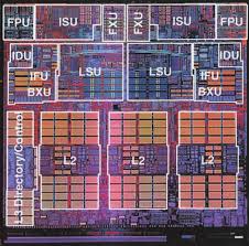
Archive for the ‘Reverse Engineer Microcontroller’ Category
 Restore AVR Microcomputer ATTINY44 Eeprom Code
We can restore AVR microcomputer ATTINY44 eeprom code, please view the AVR microcomputer ATTINY44 features for your reference:
The 9th bit of the program counter will be forced to a ‘0’ by any instruction that writes to the PC except for GOTO. See Section 4.7 “Program Counter”.
When an I/O register is modified as a function of itself (e.g. MOVF PORTB, 1), the value used will be that value present on the pins themselves. For example, if the data latch is ‘1’ for a pin configured as input and is driven low by an external device, the data will be written back with a ‘0’.
The instruction TRIS f, where f = 6, causes the contents of the W register to be written to the tri-state latches of PORTB. A ‘1’ forces the pin to a high-impedance state and disables the output buffers before Restore AVR Microcomputer ATTINY44 Eeprom Code.
If this instruction is executed on the TMR0 register (and where applicable, d = 1), the prescaler will be cleared (if assigned to TMR0).
The PIC® microcontrollers are supported with a full range of hardware and software development tools:
· Integrated Development Environment
– MPLAB® IDE Software
· Assemblers/Compilers/Linkers
– MPASMTM Assembler
– MPLAB C18 and MPLAB C30 C Compilers
– MPLINKTM Object Linker/MPLIBTM Object Librarian
– MPLAB ASM30 Assembler/Linker/Library
· Simulators
– MPLAB SIM Software Simulator
· Emulators
– MPLAB ICE 2000 In-Circuit Emulator
– MPLAB ICE 4000 In-Circuit Emulator
· In-Circuit Debugger
– MPLAB ICD 2
· Device Programmers
– PICSTART® Plus Development Programmer
– MPLAB PM3 Device Programmer
– PICkit™ 2 Development Programmer
· Low-Cost Demonstration and Development
Boards and Evaluation Kits before Restore AVR Microcomputer ATTINY44 Eeprom Code
The MPLAB IDE software brings an ease of software development previously unseen in the 8/16-bit microcontroller market. The MPLAB IDE is a Windows® operating system-based application that contains:
· A single graphical interface to all debugging tools
– Simulator
– Programmer (sold separately)
– Emulator (sold separately)
– In-Circuit Debugger (sold separately)
· A full-featured editor with color-coded context
· A multiple project manager
· Customizable data windows with direct edit of contents
· High-level source code debugging
· Visual device initializer for easy register initialization
· Mouse over variable inspection
· Drag and drop variables from source to watch windows
· Extensive on-line help if restore AVR microcomputer
· Integration of select third party tools, such as HI-TECH Software C Compilers and IAR C Compilers
The MPLAB IDE allows you to:
· Edit your source files (either assembly or C)
· One touch assemble (or compile) and download to PIC AVR microcomputer emulator and simulator tools (automatically updates all project information)
· Debug using:
– Source files (assembly or C)
– Mixed assembly and C
– Machine code
MPLAB IDE supports multiple debugging tools in a single development paradigm, from the cost-effective simulators, through low-cost in-circuit debuggers, to full-featured emulators before RECOVER MCU.
This eliminates the learning curve when upgrading to tools with increased flexibility and power.
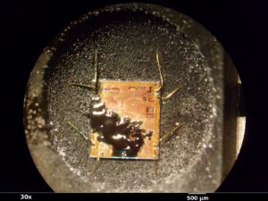
Break Mcu ATmega644PV Code
Break MCU ATmega644PV and clone heximal code from Microcontroller ATmega644PV, the code can be extracted from ATmega644PV chip program memory;
The External Interrupts are triggered by the INT7:0 pin or any of the PCINT23..0 pins. Observe that, if enabled, the interrupts will trigger even if the INT7:0 or PCINT23..0 pins are configured as outputs. This feature provides a way of generating a software interrupt.
The Pin change interrupt PCI2 will trigger if any enabled PCINT23:16 pin toggles, Pin change interrupt PCI1 if any enabled PCINT15:8 toggles and Pin change interrupts PCI0 will trigger if any enabled PCINT7..0 pin toggles. PCMSK2, PCMSK1 and PCMSK0 Registers control which pins contribute to the pin change interrupts if copy Mcu pic16c554a eeprom.
Pin change interrupts on PCINT23 ..0 are detected asynchronously. This implies that these interrupts can be used for waking the part also from sleep modes other than Idle mode.
The External Interrupts can be triggered by a falling or rising edge or a low level. This is set up as indicated in the specification for the External Interrupt Control Registers – EICRA (INT3:0) and EICRB (INT7:4). When the external interrupt is enabled and is configured as level triggered, the interrupt will trigger as long as the pin is held low if copy microcontroller pic16c76 heximal.
Note that recognition of falling or rising edge interrupts on INT7:4 requires the presence of an I/O clock, described in “Clock Systems and their Distribution” on page 39. Low level interrupts and the edge interrupt on INT3:0 are detected asynchronously.
This implies that these interrupts can be used for waking the part also from sleep modes other than Idle mode. The I/O clock is halted in all sleep modes except Idle mode.
Note that if a level triggered interrupt is used for wake-up from Power-down, the required level must be held long enough for the MCU to complete the wake-up to trigger the level interrupt when recover chip epm7064aetc100 software.
If the level disappears before the end of the Start-up Time, the MCU will still wake up, but no interrupt will be generated. The start-up time is defined by the SUT and CKSEL Fuses as described in “System Clock and Clock Options” on page 39.
The External Interrupts 3 – 0 are activated by the external pins INT3:0 if the SREG I-flag and the corresponding interrupt mask in the EIMSK is set. The level and edges on the external pins that activate the interrupts are defined in Table 31.
Edges on INT3..INT0 are registered asynchronously. Pulses on INT3:0 pins wider than the minimum pulse width given in Table 32 will generate an interrupt. Shorter pulses are not guaranteed to generate an interrupt. If low level interrupt is selected, the low level must be held until the completion of the currently executing instruction to generate an interrupt.
If enabled, a level triggered interrupt will generate an interrupt request as long as the pin is held low. When changing the ISCn bit, an interrupt can occur. Therefore, it is recommended to first disable INTn by clearing its Interrupt Enable bit in the EIMSK Register.
Then, the ISCn bit can be changed. Finally, the INTn interrupt flag should be cleared by writing a logical one to its Interrupt Flag bit (INTFn) in the EIFR Register before the interrupt is reenabled.
Reverse Engineering IC ATmega644A Firmware
Reverse Engineering IC ATmega644A and clone ATmega644A microcontroller firmware from embedded flash and eeprom memory;
If the On-chip debug system is enabled by the OCDEN Fuse and the chip enters sleep mode, the main clock source is enabled, and hence, always consumes power. In the deeper sleep modes, this will contribute significantly to the total current consumption.
There are three alternative ways to disable the OCD system: Disable the OCDEN Fuse. Disable the JTAGEN Fuse. Write one to the JTD bit in MCUCR.
During reset, all I/O Registers are set to their initial values, and the program starts execution from the Reset Vector. The instruction placed at the Reset Vector must be a JMP – Absolute Jump – instruction to the reset handling routine.
If the program never enables an interrupt source, the Interrupt Vectors are not used, and regular program firmware can be placed at these locations. This is also the case if the Reset Vector is in the Application section while the Interrupt Vectors are in the Boot section or vice versa before attack microcontroller mc68hc705p6 bin.
The circuit diagram in Figure 25 shows the reset logic. Table 23 defines the electrical parameters of the reset circuitry. The I/O ports of the AVR are immediately reset to their initial state when a reset source goes active. This does not require any clock source to be running if attack chip st62t00cb6 firmware.
After all reset sources have gone inactive, a delay counter is invoked, stretching the internal reset. This allows the power to reach a stable level before normal operation starts. The time-out period of the delay counter is defined by the user through the SUT and CKSEL Fuses. The different selections for the delay period are presented in “Clock Sources”.
The ATmega644 has five sources of reset: Power-on Reset. The MCU is reset when the supply voltage is below the Power-on Reset threshold (VPOT). External Reset. The MCU is reset when a low level is present on the RESET pin for longer than the minimum pulse length before copy mcu pic18f2480 program.
Watchdog Reset. The MCU is reset when the Watchdog Timer period expires and the Watchdog is enabled. Brown-out Reset. The MCU is reset when the supply voltage VCC is below the Brown-out Reset threshold (VBOT) and the Brown-out Detector is enabled.
JTAG AVR Reset. The MCU is reset as long as there is a logic one in the Reset Register, one of the scan chains of the JTAG system. Refer to the section “IEEE 1149.1 (JTAG) Boundary-scan” on page 301 for details.
A Power-on Reset (POR) pulse is generated by an On-chip detection circuit. The detection level is defined in Table 23. The POR is activated whenever VCC is below the detection level. The POR circuit can be used to trigger the start-up Reset, as well as to detect a failure in supply voltage.
A Power-on Reset (POR) circuit ensures that the device is reset from Power-on. Reaching the Power-on Reset threshold voltage invokes the delay counter, which determines how long the device is kept in RESET after VCC rise. The RESET signal is activated again, without any delay, when VCC decreases below the detection level.
An External Reset is generated by a low level on the RESET pin. Reset pulses longer than the minimum pulse width (see Table 23) will generate a reset, even if the clock is not running. Shorter pulses are not guaranteed to generate a reset. When the applied signal reaches the Reset Threshold Voltage – VRST – on its positive edge, the delay counter starts the MCU after the Time-out period – tTOUT – has expired.
ATmega644 has an On-chip Brown-out Detection (BOD) circuit for monitoring the VCC level during operation by comparing it to a fixed trigger level. The trigger level for the BOD can be selected by the BODLEVEL Fuses. The trigger level has a hysteresis to ensure spike free Brown-out Detection. The hysteresis on the detection level should be interpreted as VBOT+ = VBOT + VHYST/2 and VBOT- = VBOT – VHYST/2.
Recover MCU ATmega644 Code
Recover MCU ATmega644 Code from secured program memory, the code of ATmega644 will be extracted by cracking ATmega644 security fuse bit;
There are several issues to consider when trying to minimize the power consumption in an AVR controlled system. In general, sleep modes should be used as much as possible, and the sleep mode should be selected so that as few as possible of the device’s functions are operating when Recover Mcu.
All functions not needed should be disabled. In particular, the following modules may need special consideration when trying to achieve the lowest possible power consumption.
If enabled, the ADC will be enabled in all sleep modes. To save power, the ADC should be disabled before entering any sleep mode. When the ADC is turned off and on again, the next conversion will be an extended conversion. Refer to “Analog to Digital Converter” on page 274 for details on ADC operation before break IC SST89E58RD2 software.
When entering Idle mode, the Analog Comparator should be disabled if not used. When entering ADC Noise Reduction mode, the Analog Comparator should be disabled. In other sleep modes, the Analog Comparator is automatically disabled after Recover MCU dspic30f6013a firmware.
However, if the Analog Comparator is set up to use the Internal Voltage Reference as input, the Analog Comparator should be disabled in all sleep modes. Otherwise, the Internal Voltage Reference will be enabled, independent of sleep mode. Refer to “Analog Comparator” on page 271 for details on how to configure the Analog Comparator.
If the Brown-out Detector is not needed by the application, this module should be turned off. If the Brown-out Detector is enabled by the BODLEVEL Fuses, it will be enabled in all sleep modes, and hence, always consume power. In the deeper sleep modes, this will contribute significantly to the total current consumption when break Mcu at89c5131a bin.
Refer to “Brown-out Detection” on page 59 for details on how to configure the Brown-out Detector.
The Internal Voltage Reference will be enabled when needed by the Brown-out Detection, the Analog Comparator or the ADC. If these modules are disabled as described in the sections above, the internal voltage reference will be disabled and it will not be consuming power.
When turned on again, the user must allow the reference to start up before the output is used. If the reference is kept on in sleep mode, the output can be used immediately. Refer to “Internal Voltage Reference” on page 62 for details on the start-up time.
If the Watchdog Timer is not needed in the application, the module should be turned off. If the Watchdog Timer is enabled, it will be enabled in all sleep modes, and hence, always consume power. In the deeper sleep modes, this will contribute significantly to the total current consumption. Refer to “Interrupts” on page 69 for details on how to configure the Watchdog Timer.
When entering a sleep mode, all port pins should be configured to use minimum power. The most important is then to ensure that no pins drive resistive loads. In sleep modes where both the I/O clock (clkI/O) and the ADC clock (clkADC) are stopped, the input buffers of the device will be disabled.
This ensures that no power is consumed by the input logic when not needed. In some cases, the input logic is needed for detecting wake-up conditions, and it will then be enabled. Refer to the section “Digital Input Enable and Sleep Modes” on page 85 for details on which pins are enabled.
If the input buffer is enabled and the input signal is left floating or have an analog signal level close to VCC/2, the input buffer will use excessive power. For analog input pins, the digital input buffer should be disabled at all times. An analog signal level close to VCC/2 on an input pin can cause significant current even in active mode.
Digital input buffers can be disabled by writing to the Digital Input Disable Registers (DIDR2, DIDR1 and DIDR0). Refer to “Digital Input Disable Register 2 – DIDR2” on page 293, “Digital Input Disable Register 1 – DIDR1” on page 273 and “Digital Input Disable Register 0 – DIDR0” on page 293 for details.
Break Microcontroller ATmega324A Binary
Break Microcontroller ATmega324A tamper resistance system and extract embedded binary from atmega324A and decrypt ATmega324A code to c level language;
When the SM2..0 bits are written to 010, the SLEEP instruction makes the MICROCONTROLLER enter Power-down mode. In this mode, the external Oscillator is stopped, while the external interrupts, the 2-wire Serial Interface, and the Watchdog continue operating (if enabled).
Only an External Reset, a Watchdog Reset, a Brown-out Reset, 2-wire Serial Interface address match, an external level interrupt on INT7:4, an external interrupt on INT3:0, or a pin change interrupt can wake up the MICROCONTROLLER. This sleep mode basically halts all generated clocks, allowing operation of asynchronous modules only if attack microcontroller pic18f66k90 heximal.
Note that if a level triggered interrupt is used for wake-up from Power-down mode, the changed level must be held for some time to wake up the MICROCONTROLLER. Refer to “External Interrupts” on page 75 for details.
When waking up from Power-down mode, there is a delay from the wake-up condition occurs until the wake-up becomes effective. This allows the clock to restart and become stable after having been stopped. The wake-up period is defined by the same CKSEL Fuses that define the Reset Time-out period, as described in “Clock Sources” on page 40.
When the SM2..0 bits are written to 011, the SLEEP instruction makes the MICROCONTROLLER enter Power-save mode. This mode is identical to Power-down, with one exception if copy PIC18F458 MICROCONTROLLER binary:
If Timer/Counter2 is enabled, it will keep running during sleep. The device can wake up from either Timer Overflow or Output Compare event from Timer/Counter2 if the corresponding Timer/Counter2 interrupt enable bits are set in TIMSK2, and the Global Interrupt Enable bit in SREG is set.
If Timer/Counter2 is not running, Power-down mode is recommended instead of Power-save mode.
The Timer/Counter2 can be clocked both synchronously and asynchronously in Power-save mode. If the Timer/Counter2 is not using the asynchronous clock, the Timer/Counter Oscillator is stopped during sleep. If the Timer/Counter2 is not using the synchronous clock, the clock source is stopped during sleep. Note that even if the synchronous clock is running in Power-save, this clock is only available for the Timer/Counter2.
When the SM2..0 bits are 110 and an external crystal/resonator clock option is selected, the SLEEP instruction makes the MICROCONTROLLER enter Standby mode. This mode is identical to Power-down with the exception that the Oscillator is kept running. From Standby mode, the device wakes up in six clock cycles after Break MICROCONTROLLER.
When the SM2..0 bits are 111 and an external crystal/resonator clock option is selected, the SLEEP instruction makes the MICROCONTROLLER enter Extended Standby mode. This mode is identical to Power-save mode with the exception that the Oscillator is kept running.
From Extended Standby mode, the device wakes up in six clock cycles. The Power Reduction Register, PRR, provides a method to stop the clock to individual peripherals to reduce power consumption. The current state of the peripheral is frozen and the I/O registers can not be read or written.
Resources used by the peripheral when stopping the clock will remain occupied, hence the peripheral should in most cases be disabled before stopping the clock. Waking up a module, which is done by clearing the bit in PRR, puts the module in the same state as before shutdown.
Module shutdown can be used in Idle mode and Active mode to significantly reduce the overall power consumption. See “Supply Current of IO modules” on page 381 for examples. In all other sleep modes, the clock is already stopped.
Reverse Engineering IC ATmega324PV Code
Reverse Engineering IC ATmega324PV to locate the fuse bit of MCU and crack ATmega324PV for embedded memory code extraction from microcontroller ATmega324PV;
These bits define the division factor between the selected clock source and the internal system clock. These bits can be written run-time to vary the clock frequency to suit the application requirements.
As the divider divides the master clock input to the MCU, the speed of all synchronous peripherals is reduced when a division factor is used. The division factors are given in Table 20.
The CKDIV8 Fuse determines the initial value of the CLKPS bits. If CKDIV8 is unprogrammed, the CLKPS bits will be reset to “0000”.
If CKDIV8 is programmed, CLKPS bits are reset to “0011”, giving a division factor of 8 at start up. This feature should be used if the selected clock source has a higher frequency than the maximum frequency of the device at the present operating conditions after Recover chip c8051f340 firmware.
Note that any value can be written to the CLKPS bits regardless of the CKDIV8 Fuse setting. The Application software must ensure that a sufficient division factor is chosen if the selected clock source has a higher frequency than the maximum frequency of the device at the present operating conditions. The device is shipped with the CKDIV8 Fuse programmed.
Sleep modes enable the application to shut down unused modules in the MCU, thereby saving power. The AVR provides various sleep modes allowing the user to tailor the power consumption to the application’s requirements after break mcu dspic30f4011 hex.
To enter any of the five sleep modes, the SE bit in SMCR must be written to logic one and a SLEEP instruction must be executed. The SM2, SM1, and SM0 bits in the SMCR Register select which sleep mode (Idle, ADC Noise Reduction, Power-down, Power- save, or Standby) will be activated by the SLEEP instruction
The MCU is then halted for four cycles in addition to the start-up time, executes the interrupt routine, and resumes execution from the instruction following SLEEP. The contents of the Register File and SRAM are unaltered when the device wakes up from sleep. If a reset occurs during sleep mode, the MCU wakes up and executes from the Reset Vector.
Reverse Engineering Chip ATmega324 Code
Reverse Engineering Chip ATmega324 and extract ATmega324 mcu Code from embedded flash memory and eeprom memory, microcontroller ATmega324 can be unlocked;
The device can utilize a 32.768 kHz watch crystal as clock source by a dedicated Low Frequency Crystal Oscillator. The crystal should be connected as shown in Figure 22.
When this Oscillator is selected, start-up times are determined by the SUT Fuses and CKSEL0 as shown in Table 13. The calibrated internal RC Oscillator by default provides a 8.0 MHz clock. The frequency is nominal value at 3V and 25°C. The device is shipped with the CKDIV8 Fuse programmed.
See “System Clock Prescaler” on page 48 for more details. This clock may be selected as the system clock by programming the CKSEL Fuses as shown in Table If selected, it will operate with no external components before Recover IC AT89C4051 hex.
During reset, hardware loads the calibration byte into the OSCCAL Register and thereby automatically calibrates the RC Oscillator. At 3V and 25°C, this calibration gives a frequency of 8 MHz ± 1%.
The oscillator can be calibrated to any frequency in the range 7.3 – 8.1 MHz within ±1% accuracy, by changing the OSCCAL register. When this Oscillator is used as the chip clock, the Watchdog Oscillator will still be used for the Watchdog Timer and for the Reset Time-out. For more information on the pre-programmed calibration value, see the section “Calibration Byte” on page 338 before Recover microcontroller 430G2452 heximal.
The device is shipped with this option selected.
The frequency ranges are preliminary values. Actual values are TBD.
If 8 MHz frequency exceeds the specification of the device (depends on VCC), the CKDIV8 Fuse can be programmed in order to divide the internal frequency by 8. When this Oscillator is selected, start-up times are determined by the SUT Fuses as shown in Table 15 on page 46.
The Oscillator Calibration Register is used to trim the Calibrated Internal RC Oscillator to remove process variations from the oscillator frequency before break chip LPC2132FBD64 firmware.
The factory-calibrated value is automatically written to this register during chip reset, giving an oscillator frequency of 8.0 MHz at 25°C. The application software can write this register to change the oscillator frequency.
The oscillator can be calibrated to any frequency in the range 7.3 – 8.1 MHz within ±1% accuracy. Calibration outside that range is not guaranteed.
Note that this oscillator is used to time EEPROM and Flash write accesses, and these write times will be affected accordingly. If the EEPROM or Flash are written, do not calibrate to more than 8.8 MHz. Otherwise, the EEPROM or Flash write may fail.
The CAL7 bit determines the range of operation for the oscillator. Setting this bit to 0 gives the lowest frequency range, setting this bit to 1 gives the highest frequency range. The two frequency ranges are overlapping, in other words a setting of OSCCAL = 0x7F gives a higher frequency than OSCCAL = 0x80.
The CAL6..0 bits are used to tune the frequency within the selected range. A setting of 0x00 gives the lowest frequency in that range, and a setting of 0x7F gives the highest frequency in the range. Incrementing CAL6..0 by 1 will give a frequency increment of less than 2% in the frequency range 7.3 – 8.1 MHz.
The 128 kHz internal Oscillator is a low power Oscillator providing a clock of 128 kHz. The frequency is nominal at 3V and 25°C. This clock may be select as the system clock by programming the CKSEL Fuses to “11” as shown in Table 16.
When applying an external clock, it is required to avoid sudden changes in the applied clock frequency to ensure stable operation of the MCU. A variation in frequency of more than 2% from one clock cycle to the next can lead to unpredictable behavior.
If changes of more than 2% is required, ensure that the MCU is kept in Reset during the changes. Note that the System Clock Prescaler can be used to implement run-time changes of the internal clock frequency while still ensuring stable operation. Refer to “System Clock Prescaler” on page 48 for details.
Copy MCU PIC16F916 Binary
Copy MCU PIC16F916 Binary and reprograme the firmware to new microcontroller, crack MCU PIC16F916 security fuse bit and the flash content can be readout from microprocessor PIC16F916.
DEVICE OVERVIEW
The PIC16F91X/946 devices are covered by this datasheet. They are available in 28/40/44/64-pin packages. Figure 1-1 shows a block diagram of the PIC16F913/916 device, Figure 1-2 shows a block diagram of the PIC16F914/917 device, and Figure 1-3 shows a block diagram of the PIC16F946 device. Table 1-1 shows the pinout descriptions.
MEMORY ORGANIZATION
The PIC16F91X/946 has a 13-bit program counter capable of addressing a 4K x 14 program memory space for the PIC16F913/914 (0000h-0FFFh) and an 8K x 14 program memory space for the PIC16F916/917 and PIC16F946 (0000h-1FFFh). Accessing a location above the memory boundaries for the PIC16F913 and PIC16F914 will cause a wrap around within the first 4K x 14 space. The Reset vector is at 0000h and the interrupt vector is at 0004h after attack microcontroller pic18f66k90 heximal.
DATA MEMORY ORGANIZATION
The data memory is partitioned into multiple banks which contain the General Purpose Registers (GPRs) and the Special Function Registers (SFRs). Bits RP0 and RP1 are bank select bits.
Bank 0 is selected
Bank 1 is selected
Bank 2 is selected
Bank 3 is selected
Each bank extends up to 7Fh (128 bytes). The lower locations of each bank are reserved for the Special Function Registers. Above the Special Function Registers are the General Purpose Registers, implemented as static RAM. All implemented banks contain Special Function Registers. Some frequently used Special Function Registers from one bank are mirrored in another bank for code reduction and quicker access.
2.2.1
GENERAL PURPOSE REGISTER
The register file is organized as 256 x 8 bits in the PIC16F913/914, 352 x 8 bits in the PIC16F916/917 and 336 x 8 bits in the PIC16F946. Each register is accessed either directly or indirectly through the File Select for the purpose of Copy MCU pic18f458 binary
Register (FSR) (see Section 2.5 “Indirect Addressing, INDF and FSR Registers”).
SPECIAL FUNCTION REGISTERS
The Special Function Registers are registers used by the CPU and peripheral functions for controlling the desired operation of the device (see Tables 2-1, 2-2, 2-3 and 2-4). These registers are static RAM.
The Special Function Registers can be classified into two sets: core and peripheral. The Special Function Registers associated with the “core” are described in this section. Those related to the operation of the peripheral features are described in the section of that peripheral feature.
Copy Chip PIC16F777 Firmware
Copy Chip PIC16F777 Firmware from secured flash and eeprom memory, after crack PIC16F777 mcu security fuse bit and readout the firmware from microcontroller PIC16F777 program and data memory;
Copy Chip PIC16F777 Firmware
Status Register:
The Status register contains the arithmetic status of the ALU, the Reset status and the bank select bits for data memory
The Status register can be the destination for any instruction, as with any other register. If the Status register is the destination for an instruction that affects the Z, DC or C bits, then the write to these three bits is disabled. These bits are set or cleared according to the device logic.
Furthermore, the TO and PD bits are not writable, therefore, the result of an instruction with the Status register as destination may be different than intended.
For example, CLRF STATUS, will clear the upper three bits and set the Z bit. This leaves the Status register as 000u u1uu (where u = unchanged).
It is recommended, therefore, that only BCF, BSF, SWAPF and MOVWF instructions are used to alter the Status register because these instructions do not affect the Z, C or DC bits from the Status register. For other instructions not affecting any Status bits e, the result of an instruction with the Status register as destination may be different than intended after Copy Chip pic16f886 firmware.
The Program Counter (PC) is 13 bits wide. The low byte comes from the PCL register which is a readable and writable register. The upper bits (PC<12:8>) are not readable but are indirectly writable through the PCLATH register. On any Reset, the upper bits of the PC will be cleared. Figure 2-4 shows the two situations for the loading of the PC. The upper example in the figure shows how the PC is loaded on a write to PCL (PCLATH<4:0> → PCH). The lower example in the figure shows how the PC is loaded during a CALL or GOTO instruction (PCLATH<4:3> → PCH) for the purpose of Copy mcu at89c55wd bin.
The stack operates as a circular buffer. This means that after the stack has been PUSHed eight times, the ninth push overwrites the value that was stored from the first push. The tenth push overwrites the second push (and so on).
PIC16F7X7 devices are capable of addressing a con- been PUSHed eight times, the ninth push overwrites the value that was stored from the first push. The tenth push overwrites the second push (and so on). tinuous 8K word block of program memory. The CALL and GOTO instructions provide only 11 bits of address to allow branching within any 2K program memory page.
When doing a CALL or GOTO instruction, the upper 2 bits of the address are provided by PCLATH<4:3>.
Copy Microcontroller PIC16F767 Program
Copy Microcontroller PIC16F767 Program from embedded program memory, protection of mcu pic16f767 will be attacked and copy the new firmware into new MCU pic16f767;
Copy Microcontroller PIC16F767 Program from embedded program memory, protection of mcu pic16f767 will be attacked and copy the new firmware into new MCU pic16f767
MEMORY ORGANIZATION
There are two memory blocks in each of these PICmicro® MCUs. The program memory and data memory have separate buses so that concurrent access can occur and is detailed in this section. The program memory can be read internally by user code (see Section 3.0 “Reading Program Memory”) when copy P87C51X2BBD microcontroller.
Additional information on device memory may be found in the “PICmicro® Mid-Range MCU Family Reference Manual” (DS33023).
The PIC16F767 devices have a 13-bit program counter capable of addressing an 8K word x 14-bit program memory space. The PIC16F767 devices have 8K words of Flash program memory and the PIC16F767 devices have 4K words. The program memory maps for PIC16F7X7 devices are shown in Figure 2-1. Accessing a location above the physically implemented address will cause a wraparound. in the “PICmicro® Mid-Range MCU Family Reference.
The Reset vector is at 0000h and the interrupt vector is at 0004h.
The data memory is partitioned into multiple banks which contain the General Purpose Registers and the Special Function Registers. Bits RP1 (Status<6>) and RP0 (Status<5>) are the bank select bits if copy recover 430G2452 microcontroller:
Each bank extends up to 7Fh (128 bytes). The lower locations of each bank are reserved for the Special Function Registers. Above the Special Function Registers are General Purpose Registers, implemented as static RAM. All implemented banks contain Special Function Registers. Some frequently used Special Function Registers from one bank may be mirrored in another bank for code reduction and quicker access.