Archive for the ‘Reverse Engineer Microcontroller’ Category
 Copy MCU PIC32MX440F512H Binary
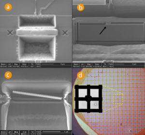
Copy MCU PIC32MX440F512H Binary and rewrite the firmware from master Microcontroller PIC32MX440F512H to blank new Microprocessor, decapsulate the MCU PIC32MX440F512H and get access to the databus is the first step of MCU cracking;
High-Performance 32-bit RISC CPU:
· MIPS32® M4K® 32-bit core with 5-stage pipeline
· 80 MHz maximum frequency
· 1.56 DMIPS/MHz (Dhrystone 2.1) performance at 0 wait state Flash access
· Single-cycle multiply and high-performance divide unit
· MIPS16e® mode for up to 40% smaller code size
· Two sets of 32 core register files (32-bit) to reduce interrupt latency
· Prefetch Cache module to speed execution
· Operating temperature range of -40ºC to +105ºC
· Operating voltage range of 2.3V to 3.6V
· 32K to 512K Flash memory (plus an additional 12 KB of boot Flash)
· 8K to 32K SRAM memory
· Pin-compatible with most PIC24/dsPIC® DSC devices
· Multiple power management modes
· Multiple interrupt vectors with individually programmable priority
· Fail-Safe Clock Monitor Mode
· Configurable Watchdog Timer with on-chip Low-Power RC Oscillator for reliable operation
Peripheral Features:
· Atomic SET, CLEAR and INVERT operation on select peripheral registers
· Up to 4-channel hardware DMA with automatic data size detection
· USB 2.0-compliant full-speed device and On-The-Go (OTG) controller
· USB has a dedicated DMA channel
· 3 MHz to 25 MHz crystal oscillator
· Internal 8 MHz and 32 kHz oscillators
· Separate PLLs for CPU and USB clocks
· Two I2C™ modules
· Two UART modules with:
– RS-232, RS-485 and LIN support
– IrDA® with on-chip hardware encoder and decoder
· Up to two SPI modules
· Parallel Master and Slave Port (PMP/PSP) with 8-bit and 16-bit data and up to 16 address lines
· Hardware Real-Time Clock and Calendar (RTCC)
· Five 16-bit Timers/Counters (two 16-bit pairs combine to create two 32-bit timers)
· Five capture inputs
· Five compare/PWM outputs
· Five external interrupt pins
· High-Speed I/O pins capable of toggling at up to 80 MHz
· High-current sink/source (18 mA/18 mA) on all I/O pins
· Configurable open-drain output on digital I/O pins
Debug Features:
· Two programming and debugging Interfaces:
– 2-wire interface with unintrusive access and real-time data exchange with application
– 4-wire MIPS® standard enhanced JTAG interface
· Unintrusive hardware-based instruction trace
· IEEE Standard 1149.2-compatible (JTAG) boundary scan
Analog Features:
· Up to 16-channel 10-bit Analog-to-Digital Converter:
– 1000 ksps conversion rate
– Conversion available during Sleep, Idle
· Two Analog Comparators
Copy IC ATmega8L Heximal
In the fast-moving world of embedded systems, accessing and analyzing firmware stored within microcontrollers is often essential for maintenance, debugging, legacy system recovery, or competitive analysis. One of the most frequently encountered chips in various industrial and consumer applications is the ATmega8L, a low-power CMOS 8-bit microcontroller based on the AVR enhanced RISC architecture. Many times, developers, engineers, or researchers need to copy IC ATmega8L heximal content to clone, replicate, or restore a program, especially when original source code is unavailable or the chip is protected by security fuses.
En el dinámico mundo de los sistemas embebidos, acceder y analizar el firmware almacenado en microcontroladores suele ser esencial para tareas de mantenimiento, depuración, recuperación de sistemas heredados o análisis de la competencia. Uno de los chips más comunes en diversas aplicaciones industriales y de consumo es el ATmega8L, un microcontrolador CMOS de 8 bits y bajo consumo basado en la arquitectura RISC mejorada por AVR. A menudo, desarrolladores, ingenieros o investigadores necesitan copiar el contenido heximal del IC ATmega8L para clonar, replicar o restaurar un programa, especialmente cuando el código fuente original no está disponible o el chip está protegido por fusibles de seguridad.
At [Your Company Name], we specialize in helping clients break, read out, and decode secured ATmega8L memory, offering reliable solutions to duplicate or unlock protected firmware for legal and technical purposes.
Copy IC Atmega8L Heximal from MCU ATmega8L flash memory, crack MCU protective system and disable its security fuse bit, the status of Microcontroller ATmega8L will be modified from locked to unlocked one
Copy IC Atmega8L Heximal from MCU ATmega8L flash memory, crack MCU ATmega8L protective system and disable its security fuse bit, the status of Microcontroller ATmega8L will be modified from locked to unlocked one;
High-performance, Low-power AVR 8-bit Microcontroller
· Advanced RISC Architecture
– 130 Powerful Instructions – Most Single-clock Cycle Execution
– 32 x 8 General Purpose Working Registers
– Fully Static Operation
– Up to 16 MIPS Throughput at 16 MHz
– On-chip 2-cycle Multiplier
High Endurance Non-volatile Memory segments
Der ATmega8L wird häufig in Automobilsystemen, industriellen Steuerungen, der Robotik und der Unterhaltungselektronik eingesetzt. Der Chip enthält internen Flash-Speicher, EEPROM und SRAM und ist über ISP (In-System Programming) programmierbar. Nach der Inbetriebnahme werden diese Bausteine jedoch häufig durch Sicherungsbits gesperrt oder verschlüsselt, um unbefugten Zugriff zu verhindern. Hier kommt unsere Expertise ins Spiel.
– 8K Bytes of In-System Self-programmable Flash program memory
– 512 Bytes EEPROM
– 1K Byte Internal SRAM
– Write/Erase Cycles: 10,000 Flash/100,000 EEPROM (1)(3)
– Data retention: 20 years at 85°C/100 years at 25°C (2)(3)
– Optional Boot Code Section with Independent Lock Bits
In-System Programming by On-chip Boot Program True Read-While-Write Operation
– Programming Lock for Software Security
Peripheral Features
– Two 8-bit Timer/Counters with Separate Prescaler, one Compare Mode
– One 16-bit Timer/Counter with Separate Prescaler, Compare Mode, and Capture Mode
– Real Time Counter with Separate Oscillator
– Three PWM Channels
– 8-channel ADC in TQFP and QFN/MLF package
Eight Channels 10-bit Accuracy
– 6-channel ADC in PDIP package
Six Channels 10-bit Accuracy
– Byte-oriented Two-wire Serial Interface
– Programmable Serial USART
– Master/Slave SPI Serial Interface
– Programmable Watchdog Timer with Separate On-chip Oscillator
– On-chip Analog Comparator
Special Microcontroller Features
– Power-on Reset and Programmable Brown-out Detection
– Internal Calibrated RC Oscillator
![Que vous ayez affaire à un microcontrôleur ATmega8L verrouillé, à une carte obsolète avec un firmware chiffré, ou que vous ayez simplement besoin de copier un fichier hexadécimal pour un projet de sauvegarde ou de duplication, [Nom de votre entreprise] est là pour vous aider. Notre équipe expérimentée peut déverrouiller, pirater et répliquer vos données embarquées avec rapidité, précision et sécurité.](https://www.ic-crack.com/wp-content/uploads/2014/04/s-l1200-3.jpg)
Que vous ayez affaire à un microcontrôleur ATmega8L verrouillé, à une carte obsolète avec un firmware chiffré, ou que vous ayez simplement besoin de copier un fichier hexadécimal pour un projet de sauvegarde ou de duplication, [Nom de votre entreprise] est là pour vous aider. Notre équipe expérimentée peut déverrouiller, pirater et répliquer vos données embarquées avec rapidité, précision et sécurité.
– Five Sleep Modes: Idle, ADC Noise Reduction, Power-save, Power-down, and Standby I/O and Packages
– 23 Programmable I/O Lines
– 28-lead PDIP, 32-lead TQFP, and 32-pad QFN/MLF Operating Voltages
– 2.7 – 5.5V (ATmega8L)
– 4.5 – 5.5V (ATmega8) Speed Grades
– 0 – 8 MHz (ATmega8L)
– 0 – 16 MHz (ATmega8)
Power Consumption at 4 Mhz, 3V, 25°C
– Active: 3.6 mA
– Idle Mode: 1.0 mA
– Power-down Mode: 0.5 µA
Extract Chip PIC16C57A Program
Extract Chip PIC16C57A Program from microcontroller PIC16C57A flash memory, and then reprogramme heximal file into blank MCU PIC16C57A for copying, unlocking microprocessor PIC16C57A secured fuse bit;
Extract Chip PIC16C57A Program from microcontroller PIC16C57A flash memory, and then reprogramme heximal file into blank MCU PIC16C57A for cloning, unlocking microprocessor PIC16C57A secured fuse bit
The Oscillator Calibration (OSCCAL) register is used to calibrate the internal 4 MHz oscillator. It contains four to six bits for calibration. Increasing the cal value increases the frequency. See Section 7.2.5 for more information on the internal oscillator if microcontroller PIC16C65B eeprom breaking.
As a program instruction is executed, the Program Counter (PC) will contain the address of the next program instruction to be executed.
The PC value is increased by one every instruction cycle, unless an instruction changes the PC. For a GOTO instruction, bits 8:0 of the PC are provided by the GOTO instruction word. The PC Latch (PCL) is mapped to PC<7:0> after Extract Chip program.
Bit 5 of the STATUS register provides page information to bit 9 of the PC For a CALL instruction, or any instruction where the PCL is the destination, bits 7:0 of the PC again are provided by the instruction word.
However, PC<8> does not come from the instruction word, but is always cleared. The Program Counter is set upon a RESET, which means that the PC addresses the last location in the last page i.e., the oscillator calibration instruction if microcontroller PIC16F677 code copying.
After executing MOVLW XX, the PC will roll over to location 00h, and begin executing user code. The STATUS register page preselect bits are cleared upon a RESET, which means that page 0 is preselected. Therefore, upon a RESET, a GOTO instruction will automatically cause the program to jump to page 0 until the value of the page bits is altered.
Microcontroller Cracking Without Part Number
Microcontroller Cracking Without Part Number
With MCU design and manufacturing technology continues to evolve, Microcontroller cracking method is also emerging, alteration on Microcontroller’s package, erase silkscreen and burn out pins of Microcontroller as well as other methods being applied on electronic devices at home and abroad, erase silkscreen on Microcontroller is the most common method.
Microcontroller Cracking Without Part Number
For such kind of Microcontroller cracking, must first get to know the exact model number of the Microcontroller, a majority of companies use observation method like assessing the external circuit to estimate the probable models of Microcontroller, due to continuous development of the industry, the limitations of this approach has been growing, mainly in the following several reasons:
1. Because Microcontroller from same company often has compatible pins (for example: MCU from PIC series and MCU of AVR series), so even determine which series of this Microcontroller generously, but still difficult to determine its concrete model;
2. Today, different companies have compatible pins of Microcontroller is also very common (such as EMC78P156 and IC16C54C, etc.), which added more difficult for us to determine the final model number of Microcontroller;
3. Because different companies have different Microcontroller programming port and verified pins distribution, especially the distribution of high-voltage VPP pin is different, so before the Microcontroller model has not been determined, random use of programmer to read the its program (which is currently the most popular approach), it is very likely to cause damage of inside content of flash and eeprom memory.
Decode Secured Atmel Chip ATmega164A Heximal
We can decode secured Atmel Chip ATMEGA164A heximal, please view the secured Atmel Chip ATMEGA164A features for your reference:
Thus, when the BOD is not enabled, after setting the AINBG bit, the user must always allow the reference to start-up before the output from the Analog Comparator is used when decode secured Atmel Chip heximal.
The bandgap reference uses typically 10 µA, and to reduce power consumption in Power-down mode, the user can avoid the three conditions above to ensure that the reference is turned off before entering Power-down mode if Decode Secured Atmel Chip ATmega164A Heximal.
The ATtiny15L has two 8-bit Interrupt Mask control registers: GIMSK (General Interrupt Mask register) and TIMSK (Timer/Counter Interrupt Mask register) before decode secured Atmel Chip heximal.
When an interrupt occurs, the Global Interrupt Enable I-bit is cleared (zero) and all interrupts are disabled. The user software can set the I-bit (one) to enable interrupts. The Ibit is set (one) when a Return from Interrupt instruction (RETI) is executed.
When the heximal Counter is vectored to the actual interrupt vector in order to execute the interrupt handling routine, hardware clears the corresponding flag that generated the interrupt.
Some of the interrupt flags can also be cleared by writing a logical “1” to the flag bit position(s) to be cleared. If an interrupt condition occurs when the corresponding interrupt enable bit is cleared (zero), the interrupt flag will be set and remembered until the interrupt is enabled, or the flag is cleared by software if Decode Secured Atmel Chip ATmega164A Heximal.
If one or more interrupt conditions occur when the global interrupt enable bit is cleared (zero), the corresponding interrupt flag(s) will be set and remembered until the global interrupt enable bit is set (one), and will be executed by order of priority.
Note that external level interrupt does not have a flag, and will only be remembered for as long as the interrupt condition is present.
Note that the Status Register is not automatically stored when entering an interrupt routine and restored when returning from an interrupt routine. This must be handled by software if BREAK IC.
Open IC PIC16F73 Memory
Open IC PIC16F73 Memory include flash and eprom by MCU cracking technique, and extract code from microcontroller PIC16F73 in the format of heximal or binary;
The DRT operates on an internal RC oscillator. The processor is kept in RESET as long as the DRT is active. The DRT delay allows VDD to rise above VDD min., and for the oscillator to stabilize.
Oscillator circuits based on crystals or ceramic resonators require a certain time after power-up to establish a stable oscillation. The on-chip DRT keeps the device in a RESET condition for approximately 18 ms after MCLR has reached a logic high (VIHMCLR) level if recover mcu atmega164pa code.
Thus, programming GP3/MCLR/VPP as MCLR and using an external RC network connected to the MCLR input is not required in most cases, allowing for savings in cost-sensitive and/or space restricted applications, as well as allowing the use of the GP3/ MCLR/VPP pin as a general purpose input.
The Device Reset time delay will vary from chip to chip due to VDD, temperature, and process variation. See AC parameters for details.
The DRT will also be triggered upon a Watchdog Timer time-out. This is particularly important for applications using the WDT to wake from SLEEP mode automatically when reverse engineering IC atmega324pv code.
The Watchdog Timer (WDT) is a free running on-chip RC oscillator which does not require any external components. This RC oscillator is separate from the external RC oscillator of the GP5/OSC1/CLKIN pin and the internal 4 MHz oscillator.
That means that the WDT will run even if the main processor clock has been stopped, for example, by execution of a SLEEP instruction. During normal operation or SLEEP, a WDT reset or wake-up reset generates a device RESET.
The TO bit (STATUS<4>) will be cleared upon a Watchdog Timer reset. The WDT can be permanently disabled by programming the configuration bit WDTE as a ’0’. Refer to the PIC16F73 Programming. Specifications to determine how to access the configuration word.
Recover IC PIC16LF506 Data
Recover IC PIC16LF506 Data from embedded program memory and data memory, the embedded flash code can be readout from PIC16LF506 MCU after crack Microcontroller PIC16F506 protection;
Figure 8-5 shows a series resonant oscillator circuit. This circuit is also designed to use the fundamental frequency of the crystal. The inverter performs a 180-degree phase shift in a series resonant oscillator circuit.
The 330 Ω resistors provide the negative feedback to bias the inverters in their linear region. For timing insensitive applications, the RC device option offers additional cost savings if Recover mcu attiny45v program data.
The RC oscillator frequency is a function of the supply voltage, the resistor (Rext) and capacitor (Cext) values, and the operating temperature. In addition to this, the oscillator frequency will vary from unit to unit due to normal process parameter variation.
Furthermore, the difference in lead frame capacitance between package types will also affect the oscillation frequency, especially for low Cext values. The user also needs to take into account variation due to tolerance of external R and C components used after break IC attiny2313 code.
Figure 8-6 shows how the R/C combination is connected to the PIC12C5XX. For Rext values below 2.2 kΩ, the oscillator operation may become unstable, or stop completely.
For very high Rext values (e.g., 1 MΩ) the oscillator becomes sensitive to noise, humidity and leakage. Thus, we recommend keeping Rext between 3 kΩ and 100 kΩ.
Although the oscillator will operate with no external capacitor (Cext = 0 pF), we recommend using values above 20 pF for noise and stability reasons before Reverse engineering microcontroller attiny4313.
With no or small external capacitance, the oscillation frequency can vary dramatically due to changes in external capacitances, such as PCB trace capacitance or package lead frame capacitance.
The Electrical Specifications sections show RC frequency variation from part to part due to normal process variation. The variation is larger for larger R (since leakage current variation will affect RC frequency more for large R) and for smaller C (since variation of input capacitance will affect RC frequency more).
Reverse Engineering IC ATmega169 Internal Memory
We can reverse engineering IC ATMEGA169 internal memory, please view the IC ATMEGA169 features for your reference:
The AVR core combines a rich instruction set with 32 general purpose working registers. All the 32 registers are directly connected to the Arithmetic Logic Unit (ALU), allowing two independent registers to be accessed in one single instruction executed in one clock cycle.
The resulting architecture is more internal memory efficient while achieving throughputs up to ten times faster than conventional CISC microcontrollers. The ATmega169 provides the following features: 16K bytes of In-System Programmable Flash with Read-While-Write capabilities, 512 bytes EEPROM, 1K byte SRAM, 54 general purpose I/O lines, 32 general purpose working registers, a JTAG interface for Boundary-scan, On-chip Debugging support and programming, a complete On-chip LCD controller with internal step-up voltage, three flexible Timer/Counters with compare modes, internal and external interrupts, a serial programmable USART, Universal Serial Interface with Start Condition Detector, an 8-channel, 10-bit ADC, a programmable Watchdog Timer with internal Oscillator, an SPI serial port, and five software selectable power saving modes when Reverse Engineering IC ATmega169 Internal Memory.
The Idle mode stops the CPU while allowing the SRAM, Timer/Counters, SPI port, and interrupt system to continue functioning. The Power-down mode saves the register contents but freezes the Oscillator, disabling all other chip functions until the next interrupt or hardware reset.
In Power-save mode, the asynchronous timer and the LCD controller continues to run, allowing the user to maintain a timer base and operate the LCD display while the rest of the device is sleeping. The ADC Noise Reduction mode stops the CPU and all I/O modules except asynchronous timer, LCD controller and ADC, to minimize switching noise during ADC conversions.
In Standby mode, the crystal/resonator Oscillator is running while the rest of the device is sleeping. This allows very fast start-up combined with low-power consumption. The device is manufactured using Atmel’s high density non-volatile memory technology if Reverse Engineering IC ATmega169 Internal Memory.
The On-chip ISP Flash allows the program memory to be reprogrammed In-System through an SPI serial interface, by a conventional non-volatile memory programmer, or by an On-chip Boot program running on the AVR core. The Boot program can use any interface to download the application program in the Application Flash memory.
Software in the Boot Flash section will continue to run while the Application Flash section is updated, providing true Read-While-Write operation. By combining an 8-bit RISC CPU with In-System Self-Programmable Flash on a monolithic chip, the Atmel ATmega169 is a powerful microcontroller that provides a highly flexible and cost effective solution to many embedded control applications.
The ATmega169 AVR is supported with a full suite of program and system development tools including: C Compilers, Macro Assemblers, Program Debugger/Simulators, In-Circuit Emulators, and Evaluation kits after Microcontroller Reverse Engineering.
Replicate Locked IC TS80C52X2 Heximal
We can replicate locked IC TS80C52X2 heximal, please view the IC TS80C52X2 features for your reference:
TEMIC TS80C52X2 is high performance CMOS ROM, OTP, EPROM and ROMless versions of the 80C51 CMOS single chip 8-bit microcontroller. The TS80C52X2 retains all features of the TEMIC 80C51 with extended ROM/EPROM capacity (8 Kbytes), 256 bytes of internal RAM, a 6-source , 4-level interrupt system, an on-chip oscilator and three timer/counters.
In addition, the TS80C52X2 has a dual data pointer, a more versatile serial channel that facilitates multiprocessor communication (EUART) and a X2 speed improvement mechanism if replicate locked IC. The fully static design of the TS80C52X2 allows to reduce system power consumption by bringing the clock frequency down to any value, even DC, without loss of data before replicate locked IC TS80C52X2 heximal.
The TS80C52X2 has 2 software-selectable modes of reduced activity for further reduction in power consumption. In the idle mode the CPU is frozen while the timers, the serial port and the interrupt system are still operating. In the power-down mode the RAM is saved and all other functions are inoperative.
The TS80C52X2 core needs only 6 clock periods per machine cycle. This feature called ”X2” provides the following advantages: Divide frequency crystals by 2 (cheaper crystals) while keeping same CPU power. Save power consumption while keeping same CPU power (oscillator power saving). Save power consumption by dividing dynamically operating frequency by 2 in operating and idle modes when replicate locked IC TS80C52X2 heximal.
Increase CPU power by 2 while keeping same crystal frequency. In order to keep the original C51 compatibility, a divider by 2 is inserted between the XTAL1 signal and the main clock input of the core (phase generator). This divider may be disabled by software. The clock for the whole circuit and peripheral is first divided by two before being used by the CPU core and peripherals if replicate locked IC. This allows any cyclic ratio to be accepted on XTAL1 input. In X2 mode, as this divider is bypassed, the signals on XTAL1 must have a cyclic ratio between 40 to 60%. Figure 1. shows the clock generation block diagram. X2 bit is validated on XTAL1÷2 rising edge to avoid glitches when switching from X2 to STD mode.
Figure 2. shows the mode switching waveforms. The auto-reload mode configures timer 2 as a 16-bit timer or event counter with automatic reload. If DCEN bit in T2MOD is cleared, timer 2 behaves as in 80C52 (refer to the TEMIC 8-bit Microcontroller Hardware description) after replicate locked IC TS80C52X2 heximal.
If DCEN bit is set, timer 2 acts as an Up/down timer/counter as shown in Figure 4. In this mode the T2EX pin controls the direction of count. When T2EX is high, timer 2 counts up. Timer overflow occurs at FFFFh which sets the TF2 flag and generates an interrupt request. The overflow also causes the 16-bit value in RCAP2H and RCAP2L registers to be loaded into the timer registers TH2 and TL2.
When T2EX is low, timer 2 counts down. Timer underflow occurs when the count in the timer registers TH2 and TL2 equals the value stored in RCAP2H and RCAP2L registers. The underflow sets TF2 flag and reloads FFFFh into the timer registers. The EXF2 bit toggles when timer 2 overflows or underflows according to the the direction of the count. EXF2 does not generate any interrupt. This bit can be used to provide 17-bit resolution after RECOVER MCU.
Extract Atmel Microprocessor ATmega16PA Firmware
We can extract atmel microprocessor ATMEGA16PA firmware, please view the atmel microprocessor ATMEGA16PA features for your reference:
The TO, PD, GPWUF and CWUF bits in the STATUS register can be tested to determine if a Reset condition has been caused by a power-up condition, a MCLR, Watchdog Timer (WDT) Reset, wake-up on comparator change or wake-up on pin change.
A Brown-out Reset is a condition where device power (VDD) dips below its minimum value, but not to zero, and then recovers. The device should be reset in the event of a brown-out when extract atmel microprocessor.
To reset ATmega16pa devices when a Brown-out Reset occurs, external brown-out protection circuits may be built if Extract Atmel Microprocessor ATmega16PA Firmware.
A device may be powered down (Sleep) and later powered up (wake-up from Sleep). The Power-Down mode is entered by executing a SLEEP instruction.
If enabled, the Watchdog Timer will be cleared but keeps running, the TO bit (STATUS<4>) is set, the PD bit (STATUS<3>) is cleared and the oscillator driver is turned off after extract atmel microprocessor.
The I/O ports maintain the status they had before the SLEEP instruction was executed (driving high, driving low or high-impedance).
For lowest current consumption while powered down, the T0CKI input should be at VDD or VSS and the GP3/ MCLR/VPP pin must be at a logic high level if MCLR is enabled.
The device can wake-up from Sleep through one of the following events:
An external Reset input on GP3/MCLR/VPP pin, when configured as MCLR.
A Watchdog Timer time-out Reset (if WDT was enabled).
A change on input pin GP0, GP1 or GP3 when wake-up on change is enabled.
A comparator output change has occurred when wake-up on comparator change is enabled when Extract Atmel Microprocessor ATmega16PA Firmware.
These events cause a device Reset. The TO, PD GPWUF and CWUF bits can be used to determine the cause of device Reset. The TO bit is cleared if a WDT time-out occurred (and caused wake-up) if extract atmel microprocessor.
The PD bit, which is set on power-up, is cleared when SLEEP is invoked. The GPWUF bit indicates a change in state while in Sleep at pins GP0, GP1 or GP3 (since the last file or bit operation on GP port) after EXTRACT IC.
The CWUF bit indicates a change in the state while in Sleep of the comparator output.