Archive for the ‘Recover MCU’ Category
 Microcontroller PIC18F2439 Code Reverse Engineering
Microcontroller PIC18F2439 Code Reverse Engineering can help designer to copy source code from original Microchip locked MCU PIC18F2439 in the format of binary file or heximal data through unlock secured microprocessor PIC18F2439 fuse bit and readout embedded firmware from flash program memory and eeprom software memory;
microcontroller PIC18F2439 code reverse engineering can help designer to copy source code from original Microchip locked MCU PIC18F2439 in the format of binary file or heximal data through unlock secured microprocessor PIC18F2439 fuse bit and readout embedded firmware from flash program memory and eeprom software memory;
PIC18LF2439 devices can be operated in ten different oscillator modes when Clone IC flash. The user can program the Configuration bits which can be obtained in the process of Microcontroller PIC18F2439 Code Reverse Engineering, FOSC3:FOSC0, in Configuration Register 1H to select one of these ten modes:
1. LP Low-Power Crystal
2. XT Crystal/Resonator
3. HS High-Speed Crystal/Resonator
4. HSPLL High-Speed Crystal/Resonator with PLL Enabled
5. RC External Resistor/Capacitor with FOSC/4 Output on RA6
6. RCIO External Resistor/Capacitor with I/O on RA6
7. INTIO1 Internal Oscillator with FOSC/4 Output on RA6 and I/O on RA7
8. INTIO2 Internal Oscillator with I/O on RA6 and RA7
9. EC External Clock with FOSC/4 Output
10. ECIO External Clock with I/O on RA6

माइक्रोकंट्रोलर PIC18F2439 कोड रिवर्स इंजीनियरिंग डिजाइनर को मूल माइक्रोचिप लॉक किए गए MCU PIC18F2439 से बाइनरी फ़ाइल या हेक्सिमल डेटा के प्रारूप में अनलॉक सुरक्षित माइक्रोप्रोसेसर PIC18F2439 फ्यूज बिट और फ्लैश प्रोग्राम मेमोरी और ईप्रोम सॉफ्टवेयर मेमोरी से एम्बेडेड फर्मवेयर रीडआउट के माध्यम से स्रोत कोड की प्रतिलिपि बनाने में मदद कर सकता है;
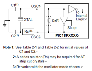
In XT, LP, HS or HSPLL Oscillator modes, a crystal or ceramic resonator is connected to the OSC1 and OSC2 pins to establish oscillation when Winbond Microcontroller W78E0516 Embedded Binary Recovering. Below Figure shows the pin connections.
The oscillator design requires the use of a parallel cut crystal. Different capacitor values may be required to produce acceptable oscillator operation after Reverse Engineering W78E52B Chip Data. The user should test the performance of the oscillator over the expected VDD and temperature range for the application.
Обратный инжиниринг кода микроконтроллера PIC18F2439 может помочь разработчику скопировать исходный код с оригинального заблокированного микроконтроллера Microchip PIC18F2439 в формате двоичного файла или шестнадцатеричных данных с помощью разблокированного защищенного бита предохранителя микропроцессора PIC18F2439 и считывания встроенной прошивки из программной флэш-памяти и программной памяти EEPROM;
When using resonators with frequencies above 3.6 MHz, the use of HS mode, rather than XT mode, is recommended for the purpose of Attack Winbond W78E051A Protected Eeprom. HS mode may be used at any VDD for which the controller is rated. If HS is selected, it is possible that the gain of the oscillator will overdrive the resonator in order to Break Nuvoton W78E054 MCU Flash Memory. Therefore, a series resistor should be placed between the OSC2 pin and the resonator. As a good starting point, the recommended value of RS is 330Ù.
مهندسی معکوس کد میکروکنترلر PIC18F2439 می تواند به طراح کمک کند تا کد منبع را از MCU PIC18F2439 قفل شده با ریزتراشه اصلی در قالب فایل باینری یا داده هگزیمال از طریق باز کردن قفل ریزپردازنده ایمن PIC18F2439 و بازخوانی سیستم عامل تعبیه شده از حافظه نرم افزار فلش و e.p.
 Restore Microprocessor Program Most Important Two Steps
Restore microprocessor program need to use Focus Ion Beam to make the necessary modification on the microprocessor program after Break IC PIC16F88 Data, and hereby we would like to introduce these two steps separately, through inject the iodin steam can have a better corruption rate of restore microprocessor program.
Restoration can produce the metal layer windows on the bottom of microprocessor program for visiting without damage the coherent structure. Through the injection of organic gas with platinic can create the new connection on the microprocessor program restore. use other chemical component like insulators can download the ion beam into the bottom metal of microprocessor program and make connection with the surface metal when restore microprocessor program without get in touch with other cover layer.
Focus ion beam can move on the surface of microprocessor program with 0.1 micron preciseness regardless the microprocessor program surface structure and evenness. Use the infrared line for imaging and can locate the transistor on the microprocessor program from it back when Break IC PIC16F715 Firmware.
After we made some necessary electrical connection and cut out on the microprocessor program for restore purpose, we need to do it’s the modification on the microprocessor program circuit pattern when restore it. As we all know, it is not necessary to have the information from databus internally of microprocessor program restore by using the microprobe technology.
Sometimes, especially for the microprocessor program itself, cut off the metal interconnection wire or break the control circuit when Recover Microcontroller PIC16F506 Binary to seal off the security protection mechanism. Focus Ion Beam is very easy to re-connect the protection security states transmission wire to the ground or power supply layer when restore microprocessor program. Although microprobe can do the same work but it won’t work if the metal wire embedded very deeply.
Microcontroller Unlocking and modification at least need to find out the restore point through the reverse engineering process which means the job can’t be done by a restoreer with less experience and well equipped facilities.
 Break IC ATTINY261 Code
Breaking IC ATTINY261 code requires specialized skills to crack or decrypt the secured microcontroller’s encrypted firmware. This protective microcomputer is designed to safeguard its flash memory and EEPROM, storing programs and software in binary or heximal formats. Reverse engineering techniques are often employed to bypass security mechanisms, allowing access to the locked source code for recovery or restoration purposes.
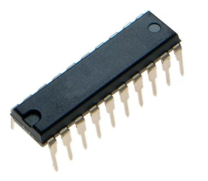
phá mã IC ATTINY261 đòi hỏi các kỹ năng chuyên biệt để bẻ khóa hoặc giải mã chương trình cơ sở được mã hóa của vi điều khiển được bảo mật. Máy vi tính bảo vệ này được thiết kế để bảo vệ bộ nhớ flash và EEPROM của nó, lưu trữ các chương trình và phần mềm ở định dạng nhị phân hoặc thập lục phân. Các kỹ thuật kỹ thuật đảo ngược thường được sử dụng để bỏ qua các cơ chế bảo mật, cho phép truy cập vào mã nguồn bị khóa cho mục đích phục hồi hoặc khôi phục
Professionals may use advanced tools to analyze the encrypted firmware, enabling the cloning or copying of the program stored in the microprocessor. This process demands a deep understanding of the ATTINY261’s architecture, as it is a highly secured MCU with features that protect its code from unauthorized access. Successfully breaking the IC ATTINY261 code enables the recovery of critical data or replication of the firmware for diagnostics or system redundancy. However, it is essential to ensure such actions comply with legal and ethical guidelines.

Break IC ATTINY261 Code
We can Break IC ATTINY261 Code, please view the IC ATTINY261 features for your reference:
High Performance, Low Power AVR® 8-Bit Microcontroller
Advanced RISC Architecture
– 123 Powerful Instructions – Most Single Clock Cycle Execution
– 32 x 8 General Purpose Working Registers
– Fully Static Operation when Break IC
Non-volatile Program and Data Memories
– 2/4/8K Byte of In-System Programmable Program Memory Flash
(ATtiny261/461/861)
Endurance: 10,000 Write/Erase Cycles
– 128/256/512 Bytes In-System Programmable EEPROM (ATtiny261)
Endurance: 100,000 Write/Erase Cycles when Reverse Engineering Microcontroller ATTINY4313 Code
– 128/256/512 Bytes Internal SRAM (ATtiny261/461/861)
– Programming Lock for Self-Programming Flash Program and EEPROM Data Security
Peripheral Features
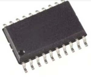
złamanie kodu IC ATTINY261 wymaga specjalistycznych umiejętności, aby złamać lub odszyfrować zaszyfrowane oprogramowanie układowe zabezpieczonego mikrokontrolera. Ten ochronny mikrokomputer jest zaprojektowany do ochrony pamięci flash i EEPROM, przechowując programy i oprogramowanie w formatach binarnych lub heksametalogowych. Techniki inżynierii wstecznej są często stosowane w celu ominięcia mechanizmów bezpieczeństwa, umożliwiając dostęp do zablokowanego kodu źródłowego w celu odzyskania lub przywrócenia
– 8/16-bit Timer/Counter with Prescaler and Two PWM Channels
– 8/10-bit High Speed Timer/Counter with Separate Prescaler after Break IC ATTINY2313 Code
3 High Frequency PWM Outputs with Separate Output Compare Registers
Programmable Dead Time Generator
– Universal Serial Interface with Start Condition Detector
– 10-bit ADC
11 Single Ended Channels
16 Differential ADC Channel Pairs
15 Differential ADC Channel Pairs with Programmable Gain (1x, 8x, 20x, 32x)
– Programmable Watchdog Timer with Separate On-chip Oscillator if Recover MCU ATTINY45V Program
– On-chip Analog Comparator
Special Microcontroller Features
– debugWIRE On-chip Debug System
– In-System Programmable via SPI Port
– External and Internal Interrupt Sources
– Low Power Idle, ADC Noise Reduction, and Power-down Modes
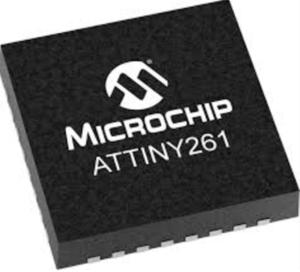
IC ATTINY261 कोड को तोड़ने के लिए सुरक्षित माइक्रोकंट्रोलर के एन्क्रिप्टेड फर्मवेयर को क्रैक या डिक्रिप्ट करने के लिए विशेष कौशल की आवश्यकता होती है। यह सुरक्षात्मक माइक्रोकंप्यूटर अपनी फ्लैश मेमोरी और EEPROM की सुरक्षा के लिए डिज़ाइन किया गया है, जो प्रोग्राम और सॉफ़्टवेयर को बाइनरी या हेक्सिमल फ़ॉर्मेट में संग्रहीत करता है। रिवर्स इंजीनियरिंग तकनीकों को अक्सर सुरक्षा तंत्र को बायपास करने के लिए नियोजित किया जाता है, जिससे रिकवरी या बहाली के उद्देश्यों के लिए लॉक किए गए स्रोत कोड तक पहुँच की अनुमति मिलती है
– Enhanced Power-on Reset Circuit
– Programmable Brown-out Detection Circuit
– Internal Calibrated Oscillator
I/O and Packages
– 16 Programmable I/O Lines after Break IC
– 20-pin PDIP, 20-pin SOIC and 32-pad MLF
Operating Voltage:
– 1.8 – 5.5V for ATtiny261
– 2.7 – 5.5V for ATtiny261
Speed Grade:
– ATtiny261V/461V/861V: 0 – 4 MHz @ 1.8 – 5.5V, 0 – 10 MHz @ 2.7 – 5.5V when Break IC
– ATtiny261/461/861: 0 – 10 MHz @ 2.7 – 5.5V, 0 – 20 MHz @ 4.5 – 5.5V
– Active Mode: 1 MHz, 1.8V: 380ìA
– Power-down Mode: 0.1ìA at 1.8V
Typical values contained in this data sheet are based on simulations and characterization of other AVR microcontrollers manufactured on the same process technology. Min and Max values will be available after the device is characterized.
The ATtiny261 is a low-power CMOS 8-bit microcontroller based on the AVR enhanced RISC architecture which can facilitate the process of Microcontroller unlocking. By executing powerful instructions in a single clock cycle, the ATtiny261 achieves throughputs approaching 1 MIPS per MHz allowing the system designer to optimize power consumption versus processing speed.
 Recover MCU PIC16HV540 Binary
Recover MCU PIC16HV540 Binary
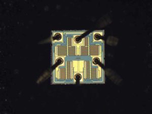
We can Recover MCU PIC16HV540 Binary, please view the MCU PIC16HV540 features for your reference:
High-Performance RISC CPU:
· Only 33 single word instructions to learn
· All instructions are single cycle (200 ns) except for program branches which are two-cycle
· Operating speed: DC – 20 MHz clock input DC – 200 ns instruction cycle
· 12-bit wide instructions
· 8-bit wide data path
· Seven special function hardware registers
· Four-level deep hardware stack
· Direct, indirect and relative addressing modes for data and instructions to Recover IC program
Peripheral Features:
· 8-bit real time clock/counter (TMR0) with 8-bit programmable prescaler
· Power-On Reset (POR)
· Brown-Out Protection
· Device Reset Timer (DRT) with short RC oscillator start-up time
· Programmable Watchdog Timer (WDT) with its own on-chip RC oscillator for reliable operation
· Sleep Timer
· 8 High Voltage I/O
· 4 Regulated I/O
· Wake up from SLEEP on-pin change
· Programmable code protection
· Power saving SLEEP mode
· Selectable oscillator options:
– RC: Low-cost RC oscillator
– XT: Standard crystal/resonator
– HS: High speed crystal/resonator
– LP: Power saving, low frequency crystal
· Glitch filtering on MCLR and pin change inputs
Recover MCU PIC16HV540 Binary
CMOS Technology:
· Selectable on-chip 3V/5V Regulator
· Low-power, high-speed CMOS EPROM technology for the purpose of Decrypt IC program
· Fully static design
· Wide-operating voltage range:
– 3.5V to 15V
· Temperature range:
– Commercial: 0°C to 70°C
– Industrial: -40°C to 85°C
· Low-power consumption
– < 2 mA typical @ 5V, 4 MHz
– 15 µA typical @ 3V, 32 kHz
– < 4.5 µA typical standby current @ 15V (with WDT disabled), 0°C to 70°C
The PIC16HV540 from Microchip Technology is a low- cost, high-performance, 8-bit, fully-static, EPROM- based CMOS microcontroller. It is pin and software compatible with the PIC16C5X family of devices. It employs a RISC architecture with only 33 single word single cycle instructions when Crack MCU. All instructions are single cycle except for program branches, which take two cycles. The PIC16HV540 delivers performance an order of magnitude higher than its competitors in the same price category after Recover MCU PIC16HV540 Binary.
The 12-bit wide instructions are highly orthogonal resulting in 2:1 code compression over other 8-bit microcontrollers in its class. The easy-to-use and easy-to-remember instruction set reduces development time significantly.
The PIC16HV540 is the first One-Time-Programmable (OTP) microcontroller with an on-chip 3 volt and 5 volt regulator. This eliminates the need for an external regulator in many applications powered from 9 Volt or 12 Volt batteries or unregulated 6 volt, 9 volt or 12 volt mains adapters.
The PIC16HV540 is ideally suited for applications that require very low standby current at high voltages. These typically require expensive low current regulators.
 Recover Microcontroller PIC16C641 Eeprom
In the world of embedded systems, microcontrollers like the PIC16C641 often store critical data in their EEPROM or flash memory, protected by secured or encrypted mechanisms. However, there are scenarios where recovering this data becomes essential, such as firmware extraction, reverse engineering, or replicating legacy systems. This is where professional MCU crack services come into play.
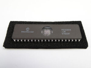
Les microcontrôleurs comme le PIC16C641 stockent souvent des données critiques dans leur EEPROM ou leur mémoire flash, protégées par des mécanismes sécurisés ou cryptés. Cependant, il existe des scénarios où la récupération de ces données devient essentielle, comme l’extraction de micrologiciels, la rétro-ingénierie ou la réplication de systèmes hérités. C’est là que les services professionnels de crackage de MCU entrent en jeu.
Using advanced techniques, experts can crack, unlock, or bypass the protected memory of microcontrollers like the PIC16C641. Whether the goal is to decrypt firmware, decode source code, or dump binary files, these services employ methods such as reverse engineering, memory attacks, or even hardware-based exploits to break through secured layers. By extracting data from EEPROM or flash memory, they can recover valuable program files, archives, or other critical information.
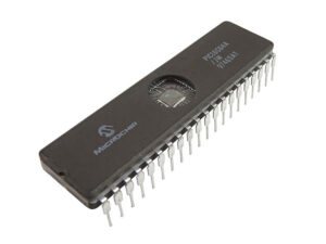
고급 기술을 사용하여 전문가는 PIC16C641과 같은 마이크로컨트롤러의 보호된 메모리를 크랙, 잠금 해제 또는 우회할 수 있습니다. 펌웨어를 해독하거나, 소스 코드를 디코딩하거나, 바이너리 파일을 덤프하는 것이 목표이든, 이러한 서비스는 리버스 엔지니어링, 메모리 공격 또는 하드웨어 기반 익스플로잇과 같은 방법을 사용하여 보안 계층을 돌파합니다. EEPROM 또는 플래시 메모리에서 데이터를 추출하여 귀중한 프로그램 파일, 아카이브 또는 기타 중요한 정보를 복구할 수 있습니다.
For those looking to replicate or clone a microcontroller, these services can also extract and replicate the entire memory content, ensuring compatibility with new or replacement chips. While ethical considerations are paramount, such capabilities are invaluable for debugging, legacy system restoration, or forensic analysis.
In summary, MCU crack services provide the tools and expertise to recover, decode, and replicate data from secured microcontrollers, unlocking the potential of even the most protected chips.
We can Recover Microcontroller PIC16C641 Eeprom, please view the Microcontroller PIC16C641 features for your reference:
High Performance RISC CPU:
· Only 35 instructions to learn
· All single-cycle instructions (200 ns), except for program branches which are two-cycle when Recover Microcontroller
· Operating speed:
– DC – 20 MHz clock input
– DC – 200 ns instruction cycle
· Interrupt capability
· 8-level deep hardware stack
· Direct, Indirect and Relative addressing modes can help to Break IC PIC12F609 Heximal
Peripheral Features:
· Up to 33 I/O pins with individual direction control
· High current sink/source for direct LED drive
· Analog comparator module with:
– Two analog comparators
– Programmable on-chip voltage reference (VREF) module
– Programmable input multiplexing from device inputs and internal voltage reference
– Comparator outputs can be output signals
· Timer0: 8-bit timer/counter with 8-bit programmable prescaler
Special Microcontroller Features:
· Power-on Reset (POR)
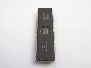
माइक्रोकंट्रोलर की नकल या क्लोनिंग करने वालों के लिए, ये सेवाएँ संपूर्ण मेमोरी सामग्री को निकाल और दोहरा सकती हैं, जिससे नए या प्रतिस्थापन चिप्स के साथ संगतता सुनिश्चित होती है। जबकि नैतिक विचार सर्वोपरि हैं, ऐसी क्षमताएँ डिबगिंग, विरासत प्रणाली बहाली या फोरेंसिक विश्लेषण के लिए अमूल्य हैं।
संक्षेप में, MCU क्रैक सेवाएँ सुरक्षित माइक्रोकंट्रोलर से डेटा को पुनर्प्राप्त करने, डिकोड करने और दोहराने के लिए उपकरण और विशेषज्ञता प्रदान करती हैं, यहाँ तक कि सबसे सुरक्षित चिप्स की क्षमता को भी अनलॉक करती हैं।
· Power-up Timer (PWRT) and Oscillator Start-up Timer (OST)
· Brown-out Reset
· Watchdog Timer (WDT) with its own on-chip RC oscillator for reliable operation
· Programmable code protection will tamper the resistance of Break IC PIC12F615 Software
· Power saving SLEEP mode
· Serial in-circuit programming (via two pins)
· Four user programmable ID locations
· Program Memory Parity Error checking circuitry with Parity Error Reset (PER) to Crack MCU
· CMOS Technology:
· Low-power, high-speed CMOS EPROM technology
· Fully static design
· Wide operating voltage range: 3.0V to 6.0V
· Commercial, Industrial and Automotive temperature ranges
· Low power consumption
– < 2.0 mA @ 5.0V, 4.0 MHz
– 15 µA typical @ 3.0V, 32 kHz
– < 1.0 µA typical standby current @ 3.0V
 Break IC PIC16C771 Firmware
The Special Function Registers are registers used by the CPU and Peripheral Modules for controlling the desired operation of the device to facilitate the process of Break IC PIC16C771 Firmware. These registers are implemented as static RAM, core (CPU) and peripheral. Those registers associated with the core functions are described in detail in this section. Those related to the operation of the peripheral features are described in detail in that peripheral feature section. For example, CLRF STATUS will clear the upper-three;
The STATUS register, shown in Register 2-1, contains the arithmetic status of the ALU, the RESET status and the bank select bits for data memory.
The STATUS register can be the destination for any instruction, as with any other register. If the STATUS register is the destination for an instruction that affects the Z, DC or C bits, then the write to these three bits is disabled.
These bits are set or cleared according to the device logic. Furthermore, the TO and PD bits are not writable. Therefore, the result of an instruction with the STATUS register as destination may be different than intended.
It is recommended, therefore, that only BCF, BSF, SWAPF and MOVWF instructions are used to alter the STATUS register, because these instructions do not affect the Z, C or DC bits from the STATUS register. For other instructions not affecting any status bits, see the ”Instruction Set Summary.
The program counter (PC) specifies the address of the instruction to fetch for execution. The PC is 13 bits wide. The low byte is called the PCL register. This register is readable and writable in order to Break IC PIC16C771 Firmware. The high byte is called the PCH register. This register contains the PC<12:8> bits and is not directly readable or writable. All updates to the PCH register occur through the PCLATH register.
PIC16C717/770/771 devices are capable of addressing a continuous 8K word block of program memory. The CALL and GOTO instructions provide only 11 bits of address to allow branching within any 2K program memory page. When doing aCALL or GOTO instruction, the upper 2 bits of the address are provided by PCLATH<4:3>. When doing a CALL or GOTO instruction, the user must ensure that the page select bits are programmed so that the desired program memory page is addressed.
A return instruction pops a PC address off the stack onto the PC register. Therefore, manipulation of the PCLATH<4:3> bits are not required for the return instructions (which POPs the address from the stack).
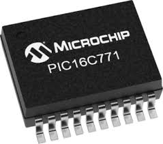
Break IC PIC16C771 Firmware
The stack allows a combination of up to 8 program calls and interrupts to occur. The stack contains the return address from this branch in program execution. Mid-range devices have an 8-level deep x 13-bit wide hardware stack. The stack space is not part of either program or data space and the stack pointer is not readable or writable which is not easy for Recover Chip PIC16F689 Flash. The PC is PUSHed onto the stack when a CALL instruction is executed or an interrupt causes a branch. The stack is POPed in the event of RETURN, RETLW or a RETFIE instruction execution. PCLATH is not modified when the stack is PUSHed or POPed.
After the stack has been PUSHed eight times, the ninth push overwrites the value that was stored from the first push. The tenth push overwrites the second push (and so on).
The INDF register is not a physical register. Addressing INDF actually addresses the register whose address is contained in the FSR register (FSR is a pointer). This is indirect addressing before Microcontroller Unlock.
Reading INDF itself indirectly (FSR = 0) will produce 00h. Writing to the INDF register indirectly results in a no-operation (although STATUS bits may be affected). A simple program to clear RAM locations 20h-2Fh using indirect addressing is shown in Example 2-1 Some pins for these I/O ports are multiplexed with an alternate function for the peripheral features on the device by PIC16F84A Microcontroller Chip Attack. In general, when a peripheral is enabled, that pin may not be used as a general purpose I/O pin.
Additional information on I/O ports may be found in the PICmicro™ Mid-Range Reference Manual, (DS33023).
PORTA is a 8-bit wide bi-directional port. The corre-analog mode of the corresponding pins. sponding data direction register is TRISA. Setting a TRISA bit (=1) will make the corresponding PORTA pin an input, i.e., put the corresponding output driver in a hi-impedance mode. Clearing a TRISA bit (=0) will make the corresponding PORTA pin an output, i.e., put the contents of the output latch on the selected pin.
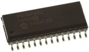
 Reverse Engineering Microcontroller PIC16F882 Heximal
We can Reverse engineering Microcontroller PIC16F882 Heximal, please view the Microcontroller PIC16F882 features for your reference:
High-Performance RISC CPU:
· Only 35 Instructions to Learn:
– All single-cycle instructions except branches
· Operating Speed:
– DC – 20 MHz oscillator/clock input
– DC – 200 ns instruction cycle
· Interrupt Capability
· 8-Level Deep Hardware Stack which will bring difficult for Break IC PIC16F621A Program
· Direct, Indirect and Relative Addressing modes
Special Microcontroller Features:
· Precision Internal Oscillator:
– Factory calibrated to ±1%
– Software selectable frequency range of 8 MHz to 31 kHz
– Software tunable
– Two-Speed Start-up mode
– Crystal fail detect for critical applications
– Clock mode switching during operation for power savings
· Power-Saving Sleep mode to Unlock Microcontroller
Reverse Engineering Microcontroller PIC16F882 Heximal
· Wide Operating Voltage Range (2.0V-5.5V)
· Industrial and Extended Temperature Range
· Power-on Reset (POR)
· Power-up Timer (PWRT) and Oscillator Start-up Timer (OST)
· Brown-out Reset (BOR) with Software Control Option
· Enhanced Low-Current Watchdog Timer (WDT) with On-Chip Oscillator (software selectable nominal 268 seconds with full prescaler) with software enable to help to resist Reverse Engineering Microcontroller PIC16C620 Code
· Multiplexed Master Clear with Pull-up/Input Pin
· Programmable Code Protection
· High Endurance Flash/EEPROM Cell:
– 100,000 write Flash endurance
– 1,000,000 write EEPROM endurance
– Flash/Data EEPROM retention: > 40 years
· Program Memory Read/Write during run time by Recover MCU PIC16F873 Archive
· In-Circuit Debugger (on board)
 Attack MCU PIC16F636 Binary
Attack MCU PIC16F636 Binary
Timer1 Operation in Asynchronous Counter Mode can greatly facilitate the process of Attack MCU PIC16F636 Binary.
If control bit T1SYNC (T1CON<2>) is set, the external clock input is not synchronized. The timer continues to increment asynchronous to the internal phase clocks. The timer will continue to run during SLEEP and can generate an interrupt on overflow, which will wake-up the processor. However, special precautions in software are needed to read/write the timer.
Timer1 Oscillator
A crystal oscillator circuit is built-in between pins OSC1 (input) and OSC2 (amplifier output). It is enabled by setting control bit T1OSCEN (T1CON<3>). The oscillator is a low power oscillator rated up to 32 kHz. It will continue to run during SLEEP. It is primarily intended for a 32 kHz crystal. Table 9-2 shows the capacitor selection for the Timer1 oscillator. The Timer1 oscillator is shared with the system LP oscillator. Thus, Timer1 can use this mode only when the system clock is derived from the internal oscillator.
Asynchronous Counter Mode.
As with the system LP oscillator, the user must provide a software time delay to ensure proper oscillator start-up.
TRISA5 and TRISA4 bits are set when the Timer1 oscillator is enabled. RA5 and RA4 read as ‘0’ and TRISA5 and TRISA4 bits read as ‘1’
The Timer1 oscillator is shared with the system LP oscillator. Thus, Timer1 can use this mode only when the system clock is derived from the internal oscillator.
Reading TMR1H or TMR1L, while the timer is running from an external asynchronous clock, will ensure a valid read (taken care of in hardware). However, the user should keep in mind that reading the 16-bit timer oscillator is enabled. RA5 and RA4 read as ‘0’ and TRISA5 and TRISA4 bits read as ‘1’ in two 8-bit values itself, poses certain problems, since the timer may overflow between the reads.
For writes, it is recommended that the user simply stop the timer and write the desired values. A write contention may occur by writing to the timer registers, while the register is incrementing. This may produce an unpredictable value in the timer register before CLONE IC.
Reading the 16-bit value requires some care. Examples 12-2 and 12-3 in the PICmicro™ Mid-Range MCU Family Reference Manual (DS33023) show how to read and write Timer1 when it is running in Asynchronous mode.
 Attack MCU PIC16F676 Code
Attack MCU PIC16F676 Code
This document contains device specific information for the PIC16F676. Additional information may be found in the PICmicroTM Mid-Range Reference Manual (DS33023) from Attack MCU PIC16F676 Code, which may be obtained from your local Microchip Sales Representative or downloaded from the Microchip web site.
The Reference Manual should be considered a complementary document to this Data Sheet and is highly recommended reading for a better understanding of the device architecture and operation of the peripheral modules.
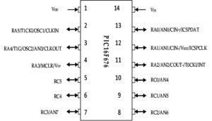
The PIC16F630 and PIC16F676 devices are covered by this Data Sheet. They are identical, except the PIC16F676 has a 10-bit A/D converter. They come in 14-pin PDIP, SOIC and TSSOP packages. Figure 1-1 shows a block diagram of the PIC16F630/676 devices. Table 1-1 shows the pinout description.
PROGRAM MEMORY ORGANIZATION
The PIC16F630/676 devices have a 13-bit program counter capable of addressing an 8K x 14 program memory space. Only the first 1K x 14 (0000h – 03FFh) for the PIC16F630/676 devices is physically implemented. Accessing a location above these boundaries will cause a wrap around within the first 1K x 14 space.
The RESET vector is at 0000h and the interrupt vector is at 0004h.
The data memory (see Figure 2-2) is partitioned into two banks, which contain the General Purpose registers and the Special Function registers. The Special Function registers are located in the first 32 locations of each bank. Register locations 20h-5Fh are General Purpose registers, implemented as static RAM and are mapped across both banks. All other RAM is unimplemented and returns ‘0’ when read. RP0 (STATUS<5>) is the bank select bit after CRACK MCU code.
SPECIAL FUNCTIONS REGISTERS
The Special Function registers are registers used by the CPU and peripheral functions for controlling the desired operation of the device (see Table 2-1). These registers are static RAM.
The special registers can be classified into two sets: core and peripheral. The Special Function registers associated with the “core” are described in this section. Those related to the operation of the peripheral features are described in the section of that peripheral feature.
 Attack MCU PIC16F630 Firmware
Attack MCU PIC16F630 Firmware
Attack MCU PIC16F630 Firmware from its memory needs to take off the protection fuse bits of MCU and then set the status of MCU into unlocking, below its PIC16F630 features:
High Performance RISC CPU:
· Only 35 instructions to learn
– All single cycle instructions except branches
· Operating speed:
– DC – 20 MHz oscillator/clock input
– DC – 200 ns instruction cycle
· Interrupt capability
· 8-level deep hardware stack
· Direct, Indirect, and Relative Addressing modes
Special Microcontroller Features:
· Internal and external oscillator options
– Precision Internal 4 MHz oscillator factory calibrated to ±1%
– External Oscillator support for crystals and resonators
– 5 µs wake-up from SLEEP, 3.0V, typical
· Power saving SLEEP mode
· Wide operating voltage range – 2.0V to 5.5V
· Industrial and Extended temperature range
· Low power Power-on Reset (POR)
· Power-up Timer (PWRT) and Oscillator Start-up Timer (OST)
· Brown-out Detect (BOD)
· Watchdog Timer (WDT) with independent oscillator for reliable operation from CRACK MCU
· Multiplexed MCLR/Input-pin
· Interrupt-on-pin change
· Individual programmable weak pull-ups
· Programmable code protection
· High Endurance FLASH/EEPROM Cell
– 100,000 write FLASH endurance
– 1,000,000 write EEPROM endurance
– FLASH/Data EEPROM Retention: > 40 years
Low Power Features:
· Standby Current:
– 1 nA @ 2.0V, typical
· Operating Current:
– 8.5 µA @ 32 kHz, 2.0V, typical
– 100 µA @ 1 MHz, 2.0V, typical
· Watchdog Timer Current
– 300 nA @ 2.0V, typical
· Timer1 oscillator current:
– 4 µA @ 32 kHz, 2.0V, typical Peripheral Features
· 12 I/O pins with individual direction control
· High current sink/source for direct LED drive
· Analog comparator module with:
– Programmable on-chip comparator voltage reference (CVREF) module
– Programmable input multiplexing from device inputs
– Comparator output is externally accessible
· Analog-to-Digital Converter module (PIC16F676):
– 10-bit resolution
– Programmable 8-channel input
– Voltage reference input
· Timer0: 8-bit timer/counter with 8-bit programmable prescaler
· Enhanced Timer1:
– 16-bit timer/counter with prescaler
– External Gate Input mode
– Option to use OSC1 and OSC2 in LP mode as Timer1 oscillator, if INTOSC mode selected
· In-Circuit Serial ProgrammingTM (ICSPTM) via two pins
