Archive for the ‘Recover MCU’ Category
 Reverse Microprocessor CPU PIC18F67K22 Flash Program
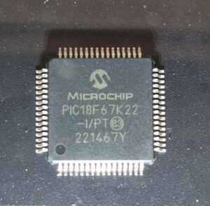
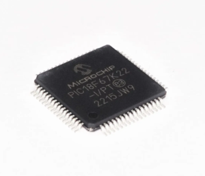
Reverse Microprocessor CPU PIC18F67K22 Flash Program is a process to unlock pic18f67k22 secured locked memory and then copy firmware heximal to new microcontroller;
The master will continue to monitor the SDAx and SCLx pins. If a Stop condition occurs, the SSPxIF bit will be set. A write to the SSPxBUF will start the transmission of data at the first data bit, regardless of where the transmitter left off when the bus collision occurred in order to carry out the protective microchip pic18f45k80 flash reverse engineering.
In Multi-Master mode, the interrupt generation on the detection of Start and Stop conditions allows the determination of when the bus is free. Control of the I2C bus can be taken when the P bit is set in the SSPxSTAT register, or the bus is Idle and the S and P bits are cleared.
El programa flash PIC18F67K22 con microprocesador seguro de ingeniería inversa es un proceso para desbloquear el sistema de protección PIC18F67K22 cifrado y extraer el contenido de la memoria integrada de la memoria flash en formato de datos binarios o archivos heximal y luego copiar el código fuente al nuevo microchip MCU PIC18F67K22;
MPLAB REAL ICE In-Circuit Emulator System is Microchip’s next generation high-speed emulator for Microchip Flash DSC and MCU devices. It debugs and programs PIC® Flash MCUs and dsPIC® Flash DSCs with the easy-to-use, powerful graphical user interface of the MPLAB Integrated Development Environment (IDE), included with each kit.
برنامج فلاش المعالج الدقيق PIC18F67K22 ذو الهندسة العكسية هو عملية لفتح نظام الحماية المشفر PIC18F67K22 واستخراج محتوى الذاكرة المضمنة من ذاكرة الفلاش بتنسيق بيانات ثنائية أو ملف سداسي ثم نسخ كود المصدر إلى شريحة MCU PIC18F67K22 الجديدة؛
The emulator is connected to the design engineer’s PC using a high-speed USB 2.0 interface and is connected to the target with either a connector compatible with in- circuit debugger systems (RJ11) or with the new high- speed, noise tolerant, Low-Voltage Differential Signal (LVDS) interconnection (CAT5).
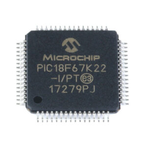
Tersine mühendislik korumalı mikroişlemci PIC18F67K22 flash programı, şifrelenmiş PIC18F67K22 koruyucu sisteminin kilidini açmaya ve gömülü bellek içeriğini ikili veri veya onaltılık dosya formatında flash bellekten çıkarmaya ve ardından kaynak kodunu yeni mikroçip MCU PIC18F67K22’ye kopyalamaya yönelik bir işlemdir;
The emulator is field upgradable through future firmware downloads in MPLAB IDE. In upcoming releases of MPLAB IDE, new devices will be supported, and new features will be added. MPLAB REAL ICE offers signifi- cant advantages over competitive emulators including low-cost, full-speed emulation, run-time variable watches, trace analysis, complex breakpoints, a rugge- dized probe interface and long (up to three meters) inter- connection cables.
 Duplicating Microchip PIC18F43K22 MCU Flash Program
Duplicating Microchip PIC18F43K22 MCU Flash Program needs to crack microcontroller pic18f43k22 security fuse bit and extract encrypted code from microprocessor.
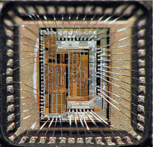
The LP, XT and HS modes support the use of quartz crystal resonators or ceramic resonators connected to OSC1 and OSC2 (Figure 2-6). The mode selects a low, medium or high gain setting of the internal inverter- amplifier to support various resonator types and speed.
LP Oscillator mode selects the lowest gain setting of the internal inverter-amplifier. LP mode current consumption is the least of the three modes. This mode is best suited to drive resonators with a low drive level specification, for example, tuning fork type crystals.
XT Oscillator mode selects the intermediate gain setting of the internal inverter-amplifier. XT mode current consumption is the medium of the three modes. This mode is best suited to drive resonators with a medium drive level specification.HS Oscillator mode offers a Medium Power (MP) and a High Power (HP) option selectable by the FOSC<3:0> bits.
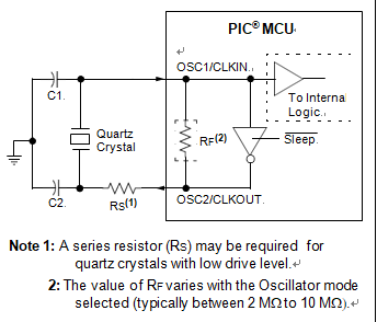
The MP selections are best suited for oscillator frequencies between 4 and 16 MHz. The HP selection has the highest gain setting of the internal inverter- amplifier and is best suited for frequencies above 16 MHz when hacking microchip mcu pic18f26k80 secured flash. HS mode is best suited for resonators that require a high drive setting.
 PIC18F4480 Microcontroller Memory Data Recovering
PIC18F4480 secured microcontroller memory data recovering can help engineer to extract embedded firmware of binary code or heximal file from locked microprocessor PIC18F4480 after crack MCU’s tamper resistance system and copy flash memory content with eeprom memory data
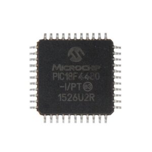
Il recupero sicuro dei dati della memoria del microcontroller PIC18F4480 può aiutare l’ingegnere a estrarre il firmware incorporato del codice binario o del file esimale dal microprocessore bloccato PIC18F4480 dopo il crack del sistema di resistenza alla manomissione dell’MCU e a copiare il contenuto della memoria flash con i dati della memoria eeprom
Large areas of data memory require an efficient addressing scheme to make rapid access to any address possible which can provide great benefit for PIC18F4480 Microcontroller Memory Data Recovering. Ideally, this means that an entire address does not need to be provided for each read or write operation. For PIC18 devices, this is accom- plished with a RAM banking scheme.
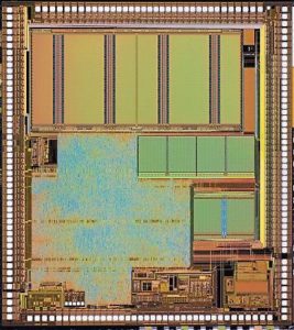
PIC18F4480 Microcontroller Memory Data Recovering
This divides the memory space into 16 contiguous banks of 256 bytes. Depending on the instruction, each location can be addressed directly by its full 12-bit address, or an 8-bit low-order address and a 4-bit Bank Pointer.
Most instructions in the PIC18F4480 instruction set make use of the Bank Pointer, known as the Bank Select Register (BSR). This SFR holds the 4 Most Significant bits of a location’s address; the instruction itself includes the 8 Least Significant bits.
Only the four lower bits of the BSR are implemented (BSR3:BSR0). The upper four bits are unused; they will always read ‘0’ and cannot be written to. The BSR can be loaded directly by using the MOVLB instruction.
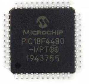
PIC18F4480 güvenli mikrodenetleyici bellek verilerinin kurtarılması, mühendisin, MCU’nun kurcalamaya karşı koruma sistemini kırdıktan ve eeprom bellek verileriyle flash bellek içeriğini kopyaladıktan sonra kilitli mikroişlemci PIC18F4480’den gömülü ikili kod veya onaltılık dosya yazılımını çıkarmasına yardımcı olabilir
The value of the BSR indicates the bank in data memory; the 8 bits in the instruction show the location in the bank and can be thought of as an offset from the bank’s lower boundary. The relationship between the BSR’s value and the bank division in data memory is shown in below Figure.
Since up to 16 registers may share the same low-order address, the user must always be careful to ensure that the proper bank is selected before performing a data read or write. For example, writing what should be program data to an 8-bit address of F9h while the BSR is 0Fh will end up resetting the program counter.
While any bank can be selected, only those banks that are actually implemented can be read or written to. Writes to unimplemented banks are ignored, while reads from unimplemented banks will return ‘0’s. Even so, the STATUS register will still be affected as if the operation was successful. The data memory map in Figure 5-5 indicates which banks are implemented.
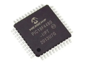
A PIC18F4480 védett mikrokontroller memóriaadatainak helyreállítása segíthet a mérnöknek a bináris kód vagy heximális fájl beágyazott firmware-jének kinyerésében a zárolt PIC18F4480 mikroprocesszorból az MCU szabotázsellenállási rendszerének feltörését követően, és a flash memória tartalmát az eeprom memóriaadatokkal másolhatja.
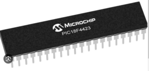
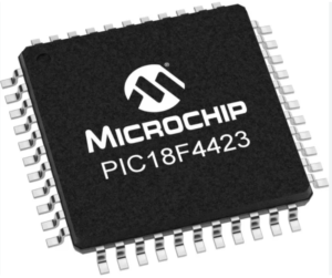
 Reverse Engineering Microchip PIC18F4423 Memory
Reverse Engineering Microchip PIC18F4423 memory read-out protection to decrypt secured microcontroller PIC18F4423, extract locked microprocessor PIC18F4423 embedded firmware of binary file or heximal source code;
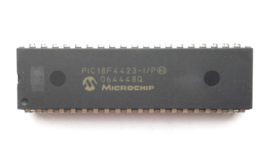
engenharia reversa Proteção de leitura de memória do Microchip PIC18F4423 para descriptografar o microcontrolador seguro PIC18F4423, extrair o firmware incorporado do microprocessador PIC18F4423 bloqueado de arquivo binário ou código-fonte heximal;
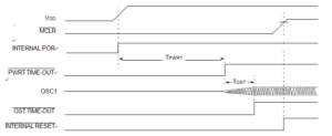
Reverse Engineering Microchip PIC18F4423 Memory can start from reseting the state of registers, knows the time-out sequence can help engineer better know the procedures of data stream flowing from one part to another:
On power-up, the time-out sequence is as follows:
1. The POR pulse clears.
2. PWRT time-out is invoked (if enabled).
3. The OST time-out is invoked. The oscillator starts at the beginning of this period.
4. PLL lock time-out (if using HSPLL mode).
The total time-out will vary based on oscillator configuration and the status of the PWRT by Attack MCU MSP430G2452IPW14R Heximal. all depict time-out sequences on power-up, with the Power-up Timer enabled and the device operating in HS Oscillator mode.
Figures 4-3 through 4-6 also apply to devices operating in XT or LP modes. For devices in RC mode and with the PWRT disabled, on the other hand, there will be no time-out at all.
обратный инжиниринг, защита считывания памяти микрочипа PIC18F4423 для расшифровки защищенного микроконтроллера PIC18F4423, извлечение встроенной прошивки заблокированного микропроцессора PIC18F4423 из двоичного файла или шестнадцатеричного исходного кода;
Since the time-outs occur from the POR pulse, if MCLR is kept low long enough, all time-outs will expire. Bring- ing MCLR high will begin execution immediately (below Figure). This is useful for testing purposes or to synchronize more than one PIC18FXXXX device operating in parallel when Attack IC TMS320F28232PGFA Software.
Most registers are unaffected by a Reset. Their status is unknown on POR and unchanged by all other Resets. The other registers are forced to a “Reset state” depending on the type of Reset that occurred.
Most registers are not affected by a WDT wake-up, since this is viewed as the resumption of normal operation. Status bits from the RCON register, RI, TO, PD, POR and BOR, are set or cleared differently in different Reset situations when Crack MCU program, as indicated in Table 4-3. These bits are used in software to determine the nature of the Reset.
रिवर्स इंजीनियरिंग माइक्रोचिप PIC18F4423 मेमोरी रीड-आउट सुरक्षा सुरक्षित माइक्रोकंट्रोलर PIC18F4423 को डिक्रिप्ट करने के लिए, बाइनरी फ़ाइल या हेक्सिमल स्रोत कोड के लॉक किए गए माइक्रोप्रोसेसर PIC18F4423 एम्बेडेड फर्मवेयर को निकालने के लिए;
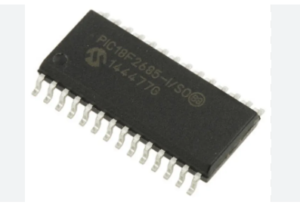
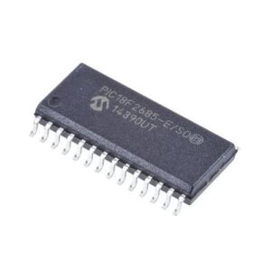
 Reverse PIC18F2685 MCU Eprom Code
Reverse engineering encrypted PIC18F2685 MCU eprom code is a process starts from unlock secured PIC18F2685 microcontroller protective system, retrieve protective embedded firmware content from PIC18F2685 microprocessor flash program memory and eeprom data memory in the format of binary code or heximal software;
Reverse engineering encrypted PIC18F2685 MCU eprom code is a process starts from unlock secured PIC18F2685 microcontroller protective system, retrieve protective embedded firmware content from PIC18F2685 microprocessor flash program memory and eeprom data memory in the format of binary code or heximal software
An exit from Sleep mode or any of the Idle modes is triggered by an interrupt from Crack MCU Program, a Reset or a WDT time-out. This section discusses the triggers that cause exits from power-managed modes from Reverse PIC18F2685 MCU Eprom Code. The clocking subsystem actions are discussed in each of the power-managed modes.
Any of the available interrupt sources can cause the device to exit from an Idle mode or the Sleep mode to a Run mode. To enable this functionality, an interrupt source must be enabled by setting its enable bit in one of the INTCON or PIE registers when Reverse Engineering MCU ATMEGA324PV heximal, The exit sequence is initiated when the corresponding interrupt flag bit is set.
L’ingénierie inverse du code EEPROM crypté du microcontrôleur PIC18F2685 est un processus qui commence par le déverrouillage du système de protection sécurisé du microcontrôleur PIC18F2685, la récupération du contenu du micrologiciel intégré de protection à partir de la mémoire de programme flash du microprocesseur PIC18F2685 et de la mémoire de données EEPROM au format de code binaire ou de logiciel hexadécimal ;
On all exits from Idle or Sleep modes by interrupt, code execution branches to the interrupt vector if the GIE/ GIEH bit (INTCON<7>) is set. Otherwise, code execution continues or resumes without branching.
A fixed delay of interval TCSD following the wake event is required when leaving Sleep and Idle modes. This delay is required for the CPU to prepare for execution after Recover MCU ATMEGA324A firmware. Instruction execution resumes on the first clock cycle following this delay.
A WDT time-out will cause different actions depending on which power-managed mode the device is in when the time-out occurs. If the device is not executing code (all Idle modes and Sleep mode), the time-out will result in an exit from the power-managed mode for the purpose of Break Microcontroller ATmega324PA binary, If the device is executing code from Reverse PIC18F2685 MCU Eprom Code (all Run modes), the time-out will result in a WDT Reset.
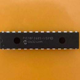
reverse engineering van gecodeerde PIC18F2685 MCU eprom-code is een proces dat begint met het ontgrendelen van het beveiligde PIC18F2685 microcontrollerbeveiligingssysteem, het ophalen van beschermende ingebedde firmware-inhoud uit het flashprogrammageheugen en eeprom-datageheugen van de PIC18F2685 microprocessor in de vorm van binaire code of heximale software;
The WDT timer and postscaler are cleared by executing a SLEEP or CLRWDT instruction, the loss of a currently selected clock source (if the Fail-Safe Clock Monitor is enabled) and modifying the IRCF bits in the OSCCON register from Break IC ATMEGA644 eeprom if the internal oscillator block is the device clock source.
 Reverse Engineering PIC18F2580 Processor Embedded Software
Reverse engineering PIC18F2580 processor embedded software starts from unlock secured microcontroller PIC18F2580 tamper resistance, copy embedded firmware of binary file or heximal data from MICROCHIP PIC18F2580 encrypted MCU flash program memory and eeprom data memory;
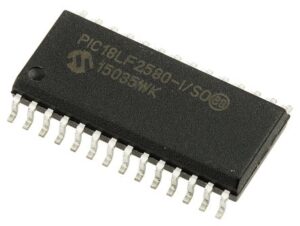
reverse engineering PIC18F2580 processor embedded software starts from unlock secured microcontroller PIC18F2580 tamper resistance, copy embedded firmware of binary file or heximal data from MICROCHIP PIC18F2580 encrypted MCU flash program memory and eeprom data memory;
This mode is entered by setting the SCS1 bit to ‘1’. Although it is ignored, it is recommended that the SCS0 bit also be cleared; this is to maintain software compatibility with future devices. When the clock source is switched to the INTOSC multiplexer when Break IC ATmega324V Protected Firmware (see below Figure), the primary oscillator is shut down and the OSTS bit is cleared by Reverse Engineering PIC18F2580 Processor Embedded Software. The IRCF bits may be modified at any time to immediately change the clock speed.
Caution should be used when modifying a single IRCF bit. If VDD is less than 3V, it is possible to select a higher clock speed than is supported by the low VDD. Improper device operation may result if the VDD/FOSC specifications are violated for the purpose of Decode Locked Microprocessor ATmega324A Source Code.
If the IRCF bits and the INTSRC bit are all clear, the INTOSC output is not enabled and the IOFS bit will remain clear; there will be no indication of the current clock source. The INTRC source is providing the device clocks.
If the IRCF bits are changed from all clear (thus, enabling the INTOSC output) or if INTSRC is set by Crack MCU Eeprom, the IOFS bit becomes set after the INTOSC output becomes stable. Clocks to the device continue while the INTOSC source stabilizes after an interval of TIOBST.
If the IRCF bits were previously at a non-zero value, or if INTSRC was set before setting SCS1 and the INTOSC source was already stable, the IOFS bit will remain set by Dump Microcontroller ATMEGA1284V Source Code.
วิศวกรรมย้อนกลับซอฟต์แวร์ฝังตัวของโปรเซสเซอร์ PIC18F2580 เริ่มจากปลดล็อคไมโครคอนโทรลเลอร์ PIC18F2580 ที่ได้รับการรักษาความปลอดภัย ป้องกันการดัดแปลง คัดลอกเฟิร์มแวร์ที่ฝังไว้ของไฟล์ไบนารีหรือข้อมูลเลขฐานสิบหกจากหน่วยความจำโปรแกรมแฟลช MCU ที่เข้ารหัส PIC18F2580 และหน่วยความจำข้อมูล EEPROM
On transitions from RC_RUN mode to PRI_RUN mode, the device continues to be clocked from the INTOSC multiplexer while the primary clock is started. When the primary clock becomes ready for Reverse Engineering PIC18F2580 Processor Embedded Software, a clock switch to the pri- mary clock occurs (see below Figure).
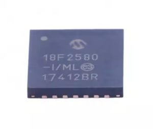
Kỹ thuật đảo ngược phần mềm nhúng của bộ vi điều khiển PIC18F2580 bắt đầu từ việc mở khóa khả năng chống giả mạo của vi điều khiển PIC18F2580 được bảo mật, sao chép chương trình cơ sở nhúng của tệp nhị phân hoặc dữ liệu thập lục phân từ bộ nhớ chương trình flash MCU được mã hóa MICROCHIP PIC18F2580 và bộ nhớ dữ liệu eeprom;
When the clock switch is complete, the IOFS bit is cleared, the OSTS bit is set and the primary clock is providing the device clock. The IDLEN and SCS bits are not affected by the switch from Reverse Engineering Chip ATmega640PV Locked Flash. The INTRC source will continue to run if either the WDT or the Fail-Safe Clock Monitor is enabled.
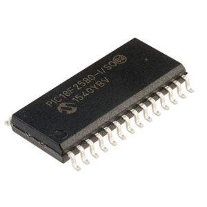
Обратное проектирование встроенного программного обеспечения процессора PIC18F2580 начинается с разблокировки защищенного микроконтроллера PIC18F2580, защиты от несанкционированного доступа, копирования встроенной прошивки двоичного файла или шестнадцатеричных данных из зашифрованной флэш-памяти программ микроконтроллера MICROCHIP PIC18F2580 и памяти данных EEPROM;
 Break Microchip PIC18F2550 MCU Memory
Break Microchip PIC18F2550 MCU memory and restore encrypted microcontroller PIC18F2550’s embedded firmware in the format of binary file or heximal data, through reverse engineering technique to crack down the protective system of locked microprocessor PIC18F2550;
break Microchip PIC18F2550 MCU memory and restore encrypted microcontroller PIC18F2550’s embedded firmware in the format of binary file or heximal data, through reverse engineering technique to crack down the protective system of locked microprocessor PIC18F2550;
PIC18F2550 devices offer a total of seven operating modes for more efficient power management by Crack MCU Firmware. These modes provide a variety of options for selective power conservation in applications where resources may be limited and Break Microchip PIC18F2550 MCU Memory (i.e., battery-powered devices).
There are three categories of power-managed modes:
• Run modes
• Idle modes
• Sleep mode
These categories define which portions of the device are clocked and sometimes, what speed. The Run and Idle modes may use any of the three available clock sources when Attack Microchip PIC18F2525 Processor Memory (primary, secondary or internal oscillator block). The Sleep mode does not use a clock source.
The power-managed modes include several power- saving features offered on previous PIC® devices.
Kilitli mikroişlemci PIC18F2550’nin koruyucu sistemini çökertmek için tersine mühendislik tekniği kullanarak Microchip PIC18F2550 MCU belleğini kırın ve şifrelenmiş mikrodenetleyici PIC18F2550’nin gömülü aygıt yazılımını ikili dosya veya onaltılık veri biçiminde geri yükleyin;
One is the clock switching feature, offered in other PIC18 devices, allowing the controller to use the Timer1 oscillator in place of the primary oscillator to facilitate the process of Reverse Engineering PIC18F2520 Controller. Also included is the Sleep mode, offered by all PIC devices, where all device clocks are stopped.
Selecting a power-managed mode requires two decisions: if the CPU is to be clocked or not and the selection of a clock source. The IDLEN bit (OSCCON<7>) controls CPU clocking, while the SCS1:SCS0 bits (OSCCON<1:0>) select the clock source for the purpose of Break PIC18F2523 CPU Memory. The individual modes, bit settings, clock sources and affected modules are summarized in below Table.
The SCS1:SCS0 bits allow the selection of one of three clock sources for power-managed modes.
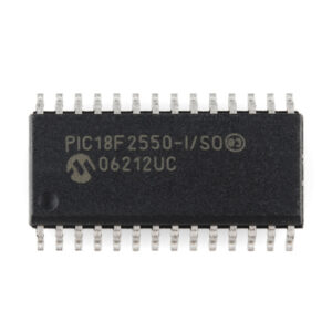
sparge memoria Microchip PIC18F2550 MCU și restaura firmware-ul încorporat al microcontrolerului criptat PIC18F2550 în format de fișier binar sau date heximale, prin tehnica de inginerie inversă pentru a distruge sistemul de protecție al microprocesorului blocat PIC18F2550;
They are: the primary clock, as defined by the FOSC3:FOSC0 Configuration bits to Microprocessor PIC18F2515 Heximal File Recovery
the secondary clock (the Timer1 oscillator)
the internal oscillator block (for RC modes)
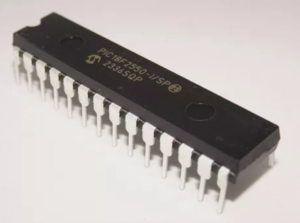
briser la mémoire du microcontrôleur Microchip PIC18F2550 et restaurer le micrologiciel intégré crypté du microcontrôleur PIC18F2550 au format de fichier binaire ou de données hexadécimales, grâce à une technique d’ingénierie inverse pour déchiffrer le système de protection du microprocesseur verrouillé PIC18F2550 ;
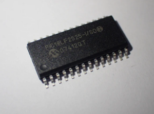
 Attack Microchip PIC18F2525 Processor Memory
Attack Microchip PIC18F2525 processor memory can help engineer restore embedded firmware in the format of binary source code or heximal data file from secured microcontroller PIC18F2525 flash program memory and eeprom data memory, then copy/write source code to new PIC18F2525 encrypted MCU;
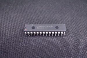
attack Microchip PIC18F2525 processor memory can help engineer restore embedded firmware in the format of binary source code or heximal data file from secured microcontroller PIC18F2525 flash program memory and eeprom data memory, then copy/write source code to new PIC18F2525 encrypted MCU;
The OSCCON register (Register 2-2) controls several aspects of the device clock’s operation which can provide critical support for Attack Microchip PIC18F2525 Processor Memory, both in full power operation and in power-managed modes to Decode Atmel AVR Processor ATMEGA169P Locked Code.
The System Clock Select bits, SCS1:SCS0, select the clock source. The available clock sources are the primary clock (defined by the FOSC3:FOSC0 Configu- ration bits), the secondary clock (Timer1 oscillator) and the internal oscillator block by Unlock Microcontroller Program. The clock source changes immediately after one or more of the bits is written to, following a brief clock transition interval. The SCS bits are cleared on all forms of Reset.
The Internal Oscillator Frequency Select bits (IRCF2:IRCF0) select the frequency output of the internal oscillator block to drive the device clock. The choices are the INTRC source, the INTOSC source (8 MHz) or one of the frequencies derived from the INTOSC postscaler for the purpose of Break Protected AVR Chip ATTINY24V Firmware (31.25 kHz to 4 MHz).
If the internal oscillator block is supplying the device clock, changing the states of these bits will have an immedi- ate change on the internal oscillator’s output. On device Resets, the default output frequency of the internal oscillator block is set at 1 MHz.
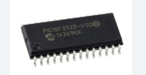
يمكن أن تساعد ذاكرة معالج PIC18F2525 من Microchip المهندس في استعادة البرامج الثابتة المضمنة بتنسيق كود المصدر الثنائي أو ملف البيانات السداسي من ذاكرة برنامج فلاش PIC18F2525 الخاصة بالميكروكنترولر المؤمنة وذاكرة بيانات EEPROM، ثم نسخ / كتابة كود المصدر إلى وحدة التحكم الدقيقة المشفرة PIC18F2525 الجديدة؛
When a nominal output frequency of 31 kHz is selected (IRCF2:IRCF0 = 000), users may choose which inter- nal oscillator acts as the source for Attack Microchip PIC18F2525 Processor Memory. This is done with the INTSRC bit in the OSCTUNE register (OSCTUNE<7>). Setting this bit selects INTOSC as a 31.25 kHz clock source by enabling the divide-by-256 output of the INTOSC postscaler.
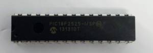
L’attacco alla memoria del processore Microchip PIC18F2525 può aiutare l’ingegnere a ripristinare il firmware incorporato nel formato di codice sorgente binario o file di dati esadecimali dalla memoria di programma flash protetta del microcontrollore PIC18F2525 e dalla memoria dati eeprom, quindi copiare/scrivere il codice sorgente sul nuovo MCU crittografato PIC18F2525;
Clearing INTSRC selects INTRC (nominally 31 kHz) as the clock source, and disables the INTOSC clock source.
This option allows users to select the tunable and more precise INTOSC as a clock source, while maintaining power savings with a very low clock speed in order to Recover ATMEL AVR ATTINY44V Flash Code. Regardless of the setting of INTSRC, INTRC always remains the clock source for features such as the Watchdog Timer and the Fail-Safe Clock Monitor.
атака Паметта на процесора Microchip PIC18F2525 може да помогне на инженера да възстанови вградения фърмуер във формат на двоичен изходен код или шестнадесетичен файл с данни от защитена флаш програмна памет PIC18F2525 на микроконтролера и памет за данни на eeprom, след което да копира/запише изходния код в нов PIC18F2525 криптиран MCU;
 Reverse Engineering PIC18F2520 Controller
Reverse engineering PIC18F2520 controller protective system and crack locked microchip MCU PIC18F2520 fuse bit in order to decrypt embedded binary or heximal firmware from PIC18F2520 microprocessor flash program memory and eeprom data memory;
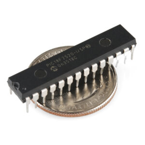
reverse engineering PIC18F2520 controller protective system and crack locked microchip MCU PIC18F2520 fuse bit in order to decrypt embedded binary or heximal firmware from PIC18F2520 microprocessor flash program memory and eeprom data memory;
The factory calibrates the internal oscillator block output (INTOSC) for 8 MHz after Crack MCU Firmware. However, this frequency may drift as VDD or temperature changes, which can affect the process of Reverse Engineering PIC18F2520 Controller operation in a variety of ways. It is possible to adjust the INTOSC frequency by modifying the value in the OSCTUNE register. This has no effect on the INTRC clock source frequency by Restore Atmel Controller ATmega88P Source Code.
Tuning the INTOSC source requires knowing when to make the adjustment, in which direction it should be made and in some cases, how large a change is needed. Three compensation techniques are discussed in Section 2.6.5.1 “Compensating with the EUSART”, Section 2.6.5.2 “Compensating with the Timers” and Section 2.6.5.3 “Compensating with the CCP Module in Capture Mode”, but other techniques may be used when Recover Protected Microcontroller ATmega169V Internal Memory.
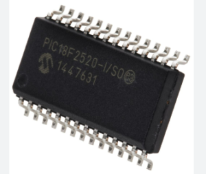
inżynieria wsteczna układu zabezpieczającego kontroler PIC18F2520 i złamanie zablokowanego bitu bezpiecznika mikroprocesora PIC18F2520 w celu odszyfrowania wbudowanego oprogramowania układowego binarnego lub heksadecymalnego z pamięci programu flash mikroprocesora PIC18F2520 i pamięci danych EEPROM;
bit 7 INTSRC: Internal Oscillator Low-Frequency Source Select bit
1 = 31.25 kHz device clock derived from 8 MHz INTOSC source (divide-by-256 enabled)
0 = 31 kHz device clock derived directly from INTRC internal oscillator bit 6 PLLEN: Frequency Multiplier PLL for INTOSC Enable bit(1)
1 = PLL enabled for INTOSC (4 MHz and 8 MHz only)
0 = PLL disabled
bit 5 Unimplemented: Read as ‘0’
bit 4-0 TUN4:TUN0: Frequency Tuning bits
01111 = Maximum frequency
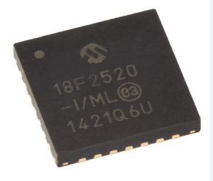
PIC18F2520 denetleyici koruma sisteminin tersine mühendisliği ve PIC18F2520 mikroişlemci flaş program belleğinden ve eeprom veri belleğinden gömülü ikili veya heksimal aygıt yazılımını şifresini çözmek için kilitli mikroçip MCU PIC18F2520 sigorta biti;
• •
• •
00001
00000 = Center frequency. Oscillator module is running at the calibrated frequency.
11111
• •
• •
10000 = Minimum frequency
An adjustment may be required when the EUSART begins to generate framing errors or receives data with errors while in Asynchronous mode by Clone Microprocessor Flash Memory Protection Method. Framing errors indicate that the device clock frequency is too high; to adjust for this, decrement the value in OSCTUNE to reduce the clock frequency by Reverse Engineering PIC18F2520 Controller.
On the other hand, errors in data may suggest that the clock speed is too low; to compensate, increment OSCTUNE to increase the clock frequency. This technique compares device clock speed to some reference clock for the purpose of Replicate Locked IC TS80C52X2 Heximal. Two timers may be used; one timer is clocked by the peripheral clock, while the other is clocked by a fixed reference source, such as the Timer1 oscillator.
 Copy PIC18F2480 MCU Locked Heximal
Copy PIC18F2480 Microchip MCU locked heximal out from secured microcontroller PIC18F2480 flash program memory and eeprom data memory needs to unlock protective PIC18F2480 microprocessor’s fuse bit, read embedded firmware out of binary file or heximal source code;
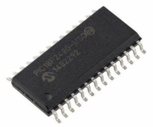
copy PIC18F2480 Microchip MCU locked heximal out from secured microcontroller PIC18F2480 flash program memory and eeprom data memory needs to unlock protective PIC18F2480 microprocessor’s fuse bit, read embedded firmware out of binary file or heximal source code;
Using the internal oscillator as the clock source eliminates the need for up to two external oscillator pins when Crack MCU Firmware, which can then be used for digital I/O and Copy PIC18F2480 MCU Locked Heximal. Two distinct configurations are available:
- In INTIO1 mode, the OSC2 pin outputs FOSC/4, while OSC1 functions as RA7 for digital input and output.
- In INTIO2 mode, OSC1 functions as RA7 and OSC2 functions as RA6, both for digital input and output.
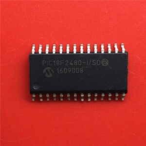
copiar PIC18F2480 Microchip MCU bloqueado heximal de la memoria de programa flash PIC18F2480 del microcontrolador protegido y la memoria de datos EEPROM necesita desbloquear el bit fusible del microprocesador PIC18F2480 protector, leer el firmware incorporado del archivo binario o código fuente heximal;
The internal oscillator block is calibrated at the factory to produce an INTOSC output frequency of 8.0 MHz when Recover Atmel AVR Controller ATmega48V Firmware.
The INTRC oscillator operates independently of the INTOSC source. Any changes in INTOSC across voltage and temperature are not necessarily reflected by changes in INTRC and vice versa.
The internal oscillator’s output has been calibrated at the factory but can be adjusted in the user’s applica- tion. This is done by writing to the OSCTUNE register from Break Atmel AVR MCU ATmega8535L Heximal.
When the OSCTUNE register is modified, the INTOSC frequency will begin shifting to the new frequency. The INTOSC clock will stabilize within 1 ms. Code execu- tion continues during this shift after Break IC ATmega88V Internal Flash. There is no indication that the shift has occurred.
скопируйте заблокированный шестнадцатеричный код микроконтроллера PIC18F2480 из защищенного микроконтроллера. Необходимо разблокировать защитный бит предохранителя микропроцессора PIC18F2480 во флэш-памяти программ и памяти данных EEPROM, считать встроенную прошивку из двоичного файла или шестнадцатеричного исходного кода;
The OSCTUNE register also implements the INTSRC and PLLEN bits, which control certain features of the internal oscillator block. The INTSRC bit allows users to select which internal oscillator provides the clock source when the 31 kHz frequency option is selected when Restore Microprocessor Program Most Important Two Steps. This is covered in greater detail in Section 2.7.1 “Oscillator Control Register”. The PLLEN bit controls the operation of the frequency multiplier, PLL, in Internal Oscillator modes.
