Archive for the ‘Recover MCU’ Category
 Recover Embedded Microprocessor MSP430G2131 Flash Software
Recover Embedded Microprocessor MSP430G2131 Flash Software is extract the locked firmware from mcu msp430g2131 flash memory after crack texas instrument msp430g2131 flash memory fuse bit;
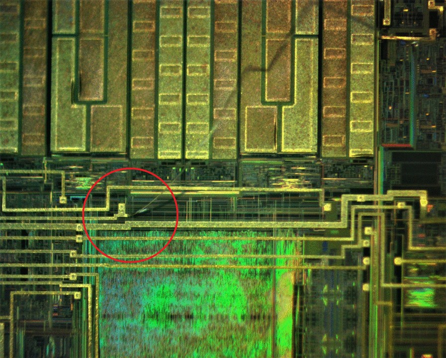
The MSP430 bootstrap loader (BSL) enables users to program the flash memory or RAM using a UART serial interface. Access to the MSP430 memory via the BSL is protected by user-defined password which can provide convenience for breaking msp430g2452 microcontroller flash memory. For complete description of the features of the BSL and its implementation, see the MSP430 Programming Via the Bootstrap Loader User’s Guide.
फ्लैश सॉफ्टवेयर MSP430G2131 एम्बेडेड माइक्रोप्रोसेसर पुनर्प्राप्त करें टेक्सास उपकरण एमएसपी 430 जी 2131 फ्लैश मेमोरी फ्यूज बिट को क्रैक करने के बाद एमसीयू एमएसपी 430 जी 2131 फ्लैश मेमोरी से लॉक किए गए फर्मवेयर को निकालता है;
The flash memory can be programmed via the JTAG port, the bootstrap loader, or in-system by the CPU. The CPU can perform single-byte and single-word writes to the flash memory. Features of the flash memory include:
- Flash memory has n segments of main memory and four segments of information memory (A to D) of 64 bytes each. Each segment in main memory is 512 bytes in size.
- Segments 0 to n may be erased in one step, or each segment may be individually erased.
- Segments A to D can be erased individually, or as a group with segments 0 to n. Segments A to D are also called information memory.
Segment A contains calibration data. After reset, segment A is protected against programming and erasing by attacking ti mcu cpu msp430g2544 flash memory. It can be unlocked, but care should be taken not to erase this segment if the device-specific calibration data is required.
 Microchip Microprocessor PIC18F85K22 Flash Memory Content Recovery
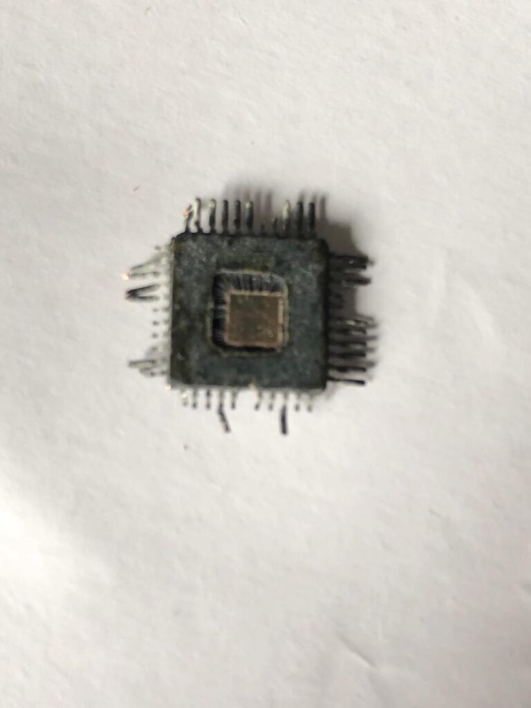
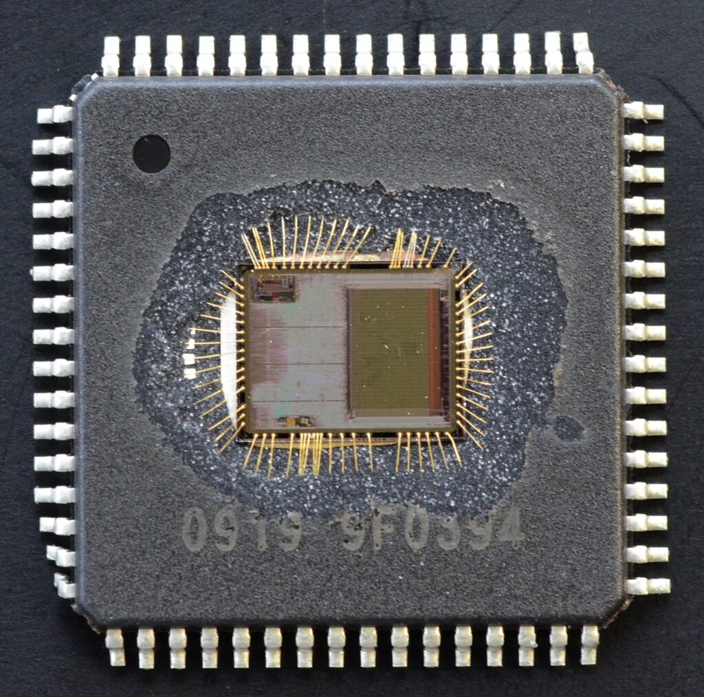
Microchip Microprocessor PIC18F85K22 Flash Memory Content Recovery will start from delayer the MCU and remove fuse bit protection over the memory by crack MCU through focus ion beam, and extract embedded firmware from microcontroller both flash and eeprom memory;
The sequence of events that takes place when switching from the Timer1 oscillator to the main oscillator will depend on the mode of the main oscillator. In addition to eight clock cycles of the main oscillator, additional delays may take place.
If the main oscillator is configured for an external crystal (HS, XT, LP), then the transition will take place after an oscillator start-up time (TOST) has occurred. A timing diagram, indicating the transition from the Timer1 oscillator to the main oscillator for HS, XT and LP modes
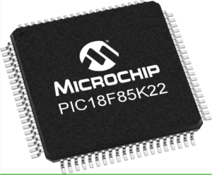
mikroçip mikroişlemci PIC18F85K22 flash bellek içerik kurtarma, MCU’nun katmanını çözmekten başlayacak ve odak iyon ışını aracılığıyla MCU’yu kırarak bellek üzerindeki sigorta biti korumasını kaldıracak ve mikrodenetleyiciden gömülü bellenimi hem flash hem de eeprom belleğinden çıkaracaktır;
If the main oscillator is configured for HS-PLL mode, an oscillator start-up time (TOST), plus an additional PLL time-out (TPLL), will occur. The PLL time-out is typically 2 ms and allows the PLL to lock to the main oscillator frequency. A timing diagram, indicating the transition from the Timer1 oscillator to the main oscillator for HS-PLL mode.
If the main oscillator is configured in the RC, RCIO, EC or ECIO modes, there is no oscillator start-up time-out. Operation will resume after eight cycles of the main oscillator have been counted by restoring microchip mcu pic18f66k80 controller embedded firmware. A timing diagram, indicating the transition from the Timer1 oscillator to the main oscillator for RC, RCIO, EC and ECIO modes.
мікрочіп мікропроцесор PIC18F85K22 відновлення вмісту флеш-пам’яті почнеться з дешарування MCU і зніме захист біта запобіжника над пам’яттю шляхом злому MCU через промінь фокусування іона, і витягне вбудовану прошивку з мікроконтролера як флеш, так і eeprom пам’яті;
When the device executes a SLEEP instruction, the on-chip clocks and oscillator are turned off and the device is held at the beginning of an instruction cycle (Q1 state). With the oscillator off, the OSC1 and OSC2 signals will stop oscillating. Since all the transistor switching currents have been removed, Sleep mode achieves the lowest current consumption of the device (only leakage currents). Enabling any on-chip feature that will operate during Sleep will increase the current consumed during Sleep when engineer try to recovering content from MCU.
 Restore MSP430G2352 Microcontroller Flash Memory Binary
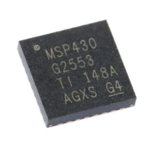
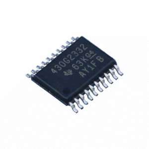
Restore MSP430G2352 Microcontroller Flash Memory Binary and copy firmware to new MCU MSP430G2352 which can provide the same functions as original version, the status of MSP430G2352 will be modified by MCU cracking from locked to unlocked one;
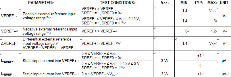
- The external reference is used during conversion to charge and discharge the capacitance array. The input capacitance, CI, is also the dynamic load for an external reference during conversion. The dynamic impedance of the reference supply should follow the recommendations on analog-source impedance to allow the charge to settle for 10-bit accuracy.
Wiederherstellen MSP430G2352 Mikrocontroller-Flash-Speicher-Binärdatei und Kopieren der Firmware auf neue MCU-MSP430G2352 die die gleichen Funktionen wie die Originalversion bieten kann, wird der Status der MSP430G2352 durch MCU-Cracking von gesperrt auf entsperrt geändert;
- The accuracy limits the minimum positive external reference voltage. Lower reference voltage levels may be applied with reduced accuracy requirements when restoring msp430g2101 flash content.
- Under this condition the external reference is internally buffered. The reference buffer is active and requires the reference buffer supply current IREFB. The current consumption can be limited to the sample and conversion period with REBURST = 1.
- The accuracy limits the maximum negative external reference voltage. Higher reference voltage levels may be applied with reduced accuracy requirements.
ripristinare MSP430G2352 binario della memoria flash del microcontrollore e copiare il firmware sul nuovo MCU MSP430G2352 che può fornire le stesse funzioni della versione originale, lo stato di MSP430G2352 verrà modificato dal cracking dell’MCU da bloccato a sbloccato;
- The accuracy limits the minimum external differential reference voltage. Lower differential reference voltage levels may be applied with reduced accuracy requirements.
 Restore Texas Instrument MSP430G2001 Microcontroller Heximal Program
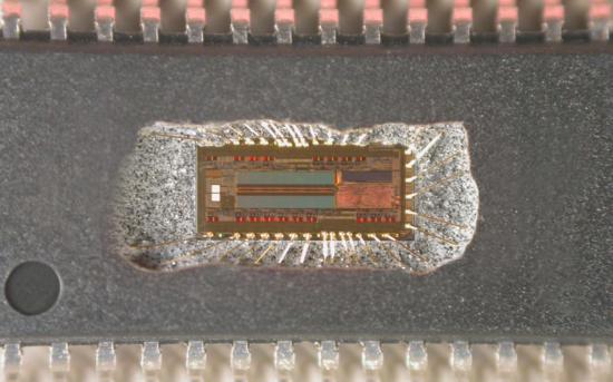
Restore Texas Instrument MSP430G2001 Microcontroller Heximal Program from embedded flash memory after crack microcontroller msp430g2001 security fuse bit and extract IC code;
The MSP430 CPU has a 16-bit RISC architecture that is highly transparent to the application. All operations, other than program-flow instructions, are performed as register operations in conjunction with seven addressing modes for source operand and four addressing modes for destination operand.
The CPU is integrated with 16 registers that provide reduced instruction execution time. The register-to-register operation execution time is one cycle of the CPU clock.
Four of the registers, R0 to R3, are dedicated as program counter, stack pointer, status register, and constant generator, respectively. The remaining registers are general-purpose registers.
Peripherals are connected to the CPU using data, address, and control buses, and can be handled with all instructions. The instruction set consists of the original 51 instructions with three formats and seven address modes and additional instructions for the expanded address range. Each instruction can operate on word and byte data to increase the success rate of msp430g2452 microcontroller flash memory protection breaking.
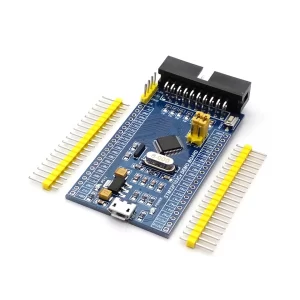
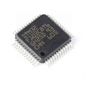
 Restore Microcontroller STM32F103C8 Flash Program Code
Restore Microcontroller STM32F103C8 Flash Program Code and copy extracted firmware to new MCU in order to make STM32F103C8 binary code microprocessor cloning;
The current consumption of the on-chip peripherals is given in Table 18. The process of Recover MCU is placed under the following conditions:
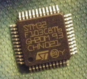
restaurar o microcontrolador STM32F103C8 código do programa flash e copiar o firmware extraído para o novo MCU, a fim de fazer STM32F103C8 clonagem de microprocessador de código binário;
- l all I/O pins are in input mode with a static value at VDD or VSS (no load)
- l all peripherals are disabled unless otherwise mentioned
- l the given value is calculated by measuring the current consumption
- – with all peripherals clocked off
- – with only one peripheral clocked on
- l ambient operating temperature and VDD supply voltage conditions summarized
External clock source characteristics includes below points:
In a given sampling window, either three or six samples of the input signal are taken to determine the validity of the signal. This is determined by the value written to GPxQSELn register to recover stmicro stm32f103c6 mcu flash content.
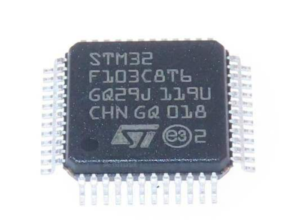
ripristinare il microcontrollore STM32F103C8 il codice del programma flash e copiare il firmware estratto sul nuovo MCU per effettuare STM32F103C8 clonazione del microprocessore in codice binario;
Case 1:
Qualification using three samples
Sampling window width = (SYSCLKOUT cycle × 2 × QUALPRD) × 2, if QUALPRD ≠ 0 Sampling window width = (SYSCLKOUT cycle) × 2, if QUALPRD = 0
Case 2:
Qualification using six samples Sampling window width = (SYSCLKOUT cycle × 2 × QUALPRD) × 5, if QUALPRD ≠ 0 Sampling window width = (SYSCLKOUT cycle) × 5, if QUALPRD = 0
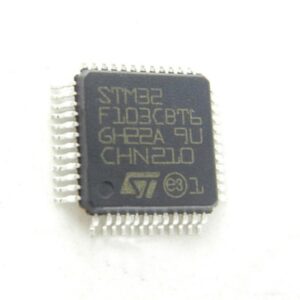
 Recovering ARM Microprocessor STM32F103CB Flash Program
Recovering ARM Microprocessor STM32F103CB Flash Program after crack mcu stm32f103cb security fuse bit and disable the protection over the memory content, copy extracted firmware to new MCU;
The low-speed external (LSE) clock can be supplied with a 32.768 kHz crystal/ceramic resonator oscillator by Crack STM32F103CB Microcontroller Flash Memory. All the information given in this paragraph are based on characterization results obtained with typical external components specified in below Table.
In the application, the resonator and the load capacitors have to be placed as close as possible to the oscillator pins in order to minimize output distortion and startup stabilization time. Refer to the crystal resonator manufacturer for more details on the resonator characteristics when break arm mcu stm32f101cb flash memory (frequency, package, accuracy).
For CL1 and CL2 it is recommended to use high-quality ceramic capacitors in the 5 pF to 15 pF range selected to match the requirements of the crystal or resonator when Break IC Flash. CL1 and CL2, are usually the same size. The crystal manufacturer typically specifies a load capacitance which is the series combination of CL1 and CL2.
 Restoring ARM Microcontroller STM32F103C4 Flash Binary
Restoring ARM Microcontroller STM32F103C4 Flash Binary after crack locked mcu stm32f103c4 security fuse bit and copy extracted firmware to new Microcontroller;
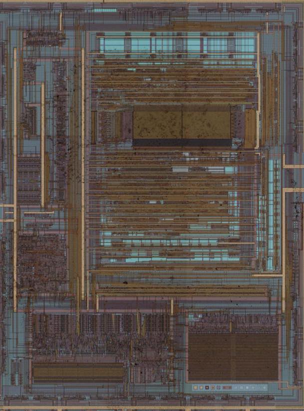
The temperature sensor has to generate a voltage that varies linearly with temperature to Recover MCU content. The conversion range is between 2 V < VDDA < 3.6 V. The temperature sensor is internally connected to the ADC1_IN16 input channel which is used to convert the sensor output voltage into a digital value.
The ARM SWJ-DP Interface is embedded, and is a combined JTAG and serial wire debug port that enables either a serial wire debug or a JTAG probe to be connected to the target of STMicro STM32F101RB MCU flash memory breaking. The JTAG TMS and TCK pins are shared respectively with SWDIO and SWCLK and a specific sequence on the TMS pin is used to switch between JTAG-DP and SW-DP.
Unless otherwise specified the minimum and maximum values in the process of Unlock ARM Base STM32F101CB Microprocessor are guaranteed in the worst conditions of ambient temperature, supply voltage and frequencies by tests in production on 100% of the devices with an ambient temperature at TA = 25 °C and TA = TAmax (given by the selected temperature range).
Data based on characterization results, design simulation and/or technology characteristics are indicated in the table footnotes and are not tested in production. Based on characterization, the minimum and maximum values refer to sample tests and represent the mean value plus or minus three times the standard deviation (mean±3S).
Unless otherwise specified, typical data are based on TA = 25 °C, VDD = 3.3 V (for the 2 V £ VDD £ 3.6 V voltage range). They are given only as design guidelines and are not tested.
 Recover STMicro STM32F100R4 Processor Flash Source Code
Recover STMicro STM32F100R4 Processor Flash Source Code from locked flash memory, crack arm microcontroller stm32f100r4 tamper resistance system and readout embedded firmware from MCU;
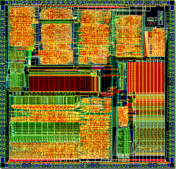
The STM32F100R4 value line embeds a nested vectored interrupt controller able to handle up to 41 maskable interrupt channels (not including the 16 interrupt lines of Cortex™-M3) and 16 priority levels which will affect Crack STM32F100R4 ARM Microcontroller process.
Closely coupled NVIC gives low latency interrupt processing
Interrupt entry vector table address passed directly to the core
Closely coupled NVIC core interface
Allows early processing of interrupts
Processing of late arriving higher priority interrupts
Support for tail-chaining
Processor state automatically saved
Interrupt entry restored on interrupt exit with no instruction overhead
This hardware block provides flexible interrupt management features with minimal interrupt latency.
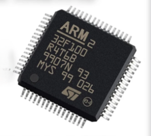
استعادة STMicro STM32F100R4 شفرة مصدر فلاش المعالجات الدقيقة من ذاكرة فلاش مقفلة ، متحكم ذراع الكراك STM32F100R4 نظام مقاومة العبث وقراءة البرامج الثابتة المضمنة من MCU ؛
The external interrupt/event controller consists of 18 edge detector lines used to generate interrupt/event requests. Each line can be independently configured to select the trigger event (rising edge, falling edge, both) and can be masked independently to provide better support in the process of restoring arm microprocessor stm32f100r8 program file.
A pending register maintains the status of the interrupt requests. The EXTI can detect an external line with a pulse width shorter than the Internal APB2 clock period. Up to 80 GPIOs can be connected to the 16 external interrupt lines.
System clock selection is performed on startup, however the internal RC 8 MHz oscillator is selected as default CPU clock on reset. An external 4-24 MHz clock can be selected, in which case it is monitored for failure. If failure is detected, the system automatically switches back to the internal RC oscillator.
लॉक ्ड फ्लैश मेमोरी से एसटीमाइक्रो STM32F100R4 माइक्रोप्रोसेसर फ्लैश सोर्स कोड पुनर्प्राप्त करें, टैम्पर प्रतिरोध प्रणाली के STM32F100R4 आर्म माइक्रोकंट्रोलर को क्रैक करें और एमसीयू से रीडआउट एम्बेडेड फर्मवेयर;
A software interrupt is generated if enabled. Similarly, full interrupt management of the PLL clock entry is available when necessary (for example on failure of an indirectly used external crystal, resonator or oscillator).
Several prescalers allow the configuration of the AHB frequency to Break IC memory, the high-speed APB (APB2) and the low-speed APB (APB1) domains. The maximum frequency of the AHB and the APB domains is 24 MHz.
 Restoring DSP Microcontroller TMS320F28067 Locked Program
Restoring DSP Microcontroller TMS320F28067 Locked Program is a process to crack mcu tms320f28067 locked flash memory and copy firmware to new microprocessor;
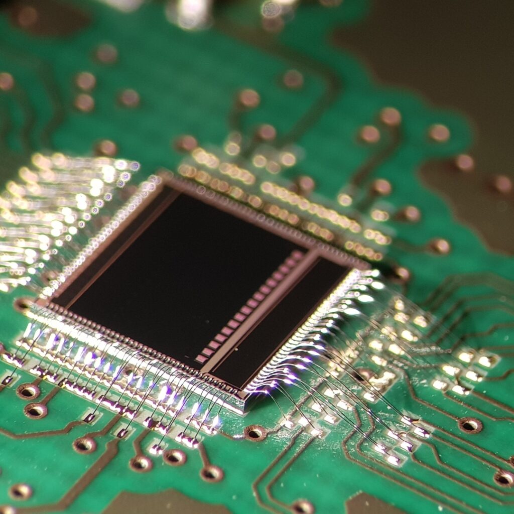
C2000™ 32-bit microcontrollers are optimized for processing, sensing, and actuation to improve closed- loop performance in real-time control applications such as industrial motor drives; solar inverters and digital power; electrical vehicles and transportation; motor control; and sensing and signal processing. The C2000 line includes the Premium performance MCUs and the Entry performance MCUs.
obnova DSP uzamčeného mikrokontroléru TMS320F28067 zamknutý program flash paměti je proces k prolomení ochranného pojistkového bitu MCU TMS320F28067 a načtení ochranného vestavěného firmwaru, zkopírování binárních dat nebo heximálního kódu do nového mikroprocesoru;
The F2806x family of microcontrollers (MCUs) provides the power of the C28x core and CLA coupled with highly integrated control peripherals in low pin-count devices.
This family is code-compatible with previous C28x-based code, and also provides a high level of analog integration which can be used to help recovering ti dsp mcu tms320f28033 flash data. An internal voltage regulator allows for single-rail operation. Enhancements have been made to the HRPWM module to allow for dual-edge control (frequency modulation).
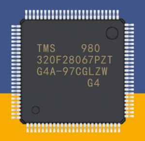
il ripristino del microcontrollore bloccato DSP Il programma di memoria flash bloccato TMS320F28067 è un processo per crackare il bit del fusibile MCU TMS320F28067 protettivo e leggere il firmware incorporato protettivo, copiare dati binari o codice esimale sul nuovo microprocessore;
Analog comparators with internal 10-bit references have been added and can be routed directly to control the ePWM outputs. The ADC converts from 0 to 3.3-V fixed full-scale range and supports ratio-metric VREFHI/VREFLO references. The ADC interface has been optimized for low overhead and latency.
 Recovering DSP TMS320F28069 Microcontroller Flash Program
Recovering DSP TMS320F28069 Microcontroller Flash Program needs to crack locked tms320f28069 flash by focus ion beam and then extract secured code from MCU;
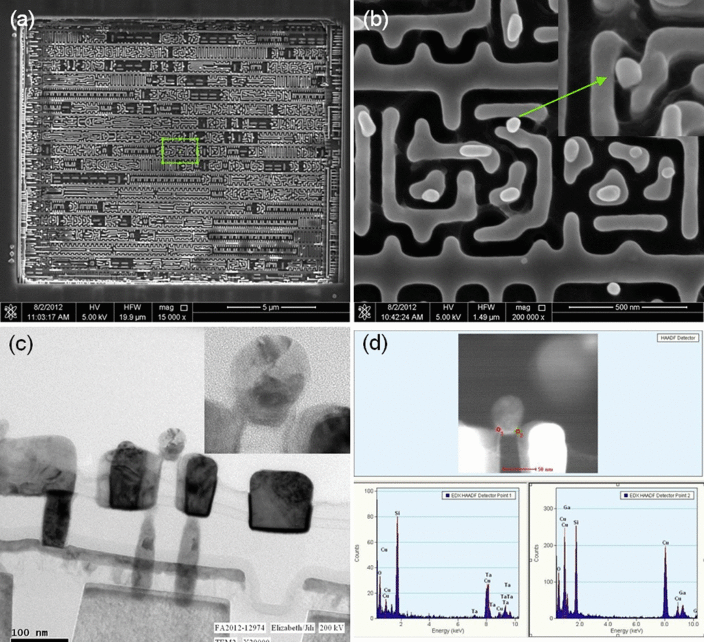
The PIE block serves to multiplex numerous interrupt sources into a smaller set of interrupt inputs. The PIE block can support up to 96 peripheral interrupts. On the F2806x, 72 of the possible 96 interrupts are used by peripherals.
The 96 interrupts are grouped into blocks of 8 and each group is fed into 1 of 12 CPU interrupt lines (INT1 to INT12). Each of the 96 interrupts is supported by its own vector stored in a dedicated RAM block that can be overwritten by the user.
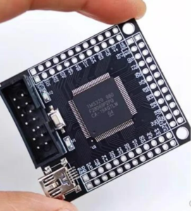
recuperați firmware-ul încorporat microcontrolerului blocat DSP TMS320F28069 din memoria flash criptată trebuie să spargeți siguranța microprocesorului TMS320F28069 blocat bit cu fascicul de ioni de focalizare și apoi extrageți codul sursă securizat în format de fișier binar sau date heximale din MCU TMS320F28069;
The vector is automatically fetched by the CPU on servicing the interrupt. Eight CPU clock cycles are needed to fetch the vector and save critical CPU registers to facilitate the process of reverse engineering TMS320F28052 flash memory code.
Hence the CPU can quickly respond to interrupt events. Prioritization of interrupts is controlled in hardware and software. Each individual interrupt can be enabled or disabled within the PIE block.
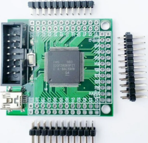
obnovit DSP TMS320F28069 vestavěný firmware vestavěného mikrokontroléru ze šifrované flash paměti potřebuje rozbít zamčený mikroprocesor TMS320F28069 pojistkový bit fokusačním iontovým paprskem a poté extrahovat zabezpečený zdrojový kód ve formátu binárního souboru nebo heximálních dat z MCU TMS320F28069;
