Archive for the ‘Recover MCU’ Category
 R8C R5F21324CNSP Microcontroller Flash Program Recovery
R8C R5F21324CNSP Microcontroller Flash Program Recovery will help engineer to restore embedded firmware inside flash memory of R5F21324CNSP, fuse bit of microprocessor R5F21324CNSP can be cracked;
This MCU integrates an internal voltage-down circuit, which is used for lowering the power supply voltage in the internal MCU to adjust automatically to the optimum level. A 4.7-μF capacitor needs to be connected between this internal voltage-down power supply (VCL pin) and VSS pin.
R8C R5F21324CNSP microcontrolador de recuperação do programa flash ajudará o engenheiro a restaurar o firmware incorporado dentro da memória flash de R5F21324CNSP, bit de fusível do microprocessador R5F21324CNSP pode ser rachado;
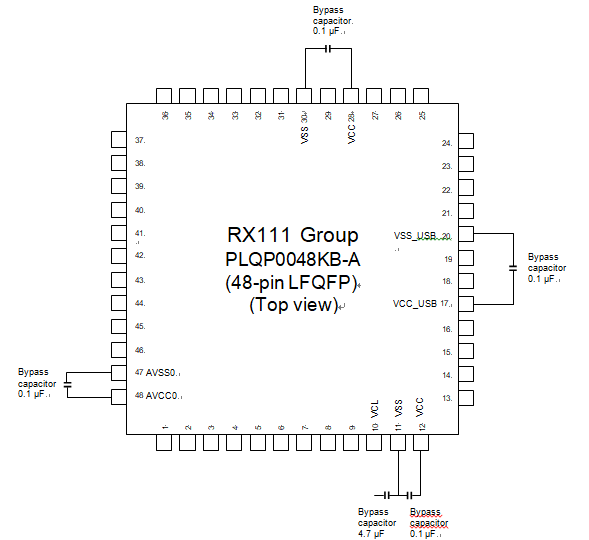
Below Figure 1 to Figure 5.64 shows how to connect external capacitors. Place an external capacitor close to the pins especially when dumping renesas r5f212a7 protected MCU flash program. Do not apply the power supply voltage to the VCL pin. Insert a multilayer ceramic capacitor as a bypass capacitor between each pair of the power supply pins. Implement a bypass capacitor to the MCU power supply pins as close as possible.
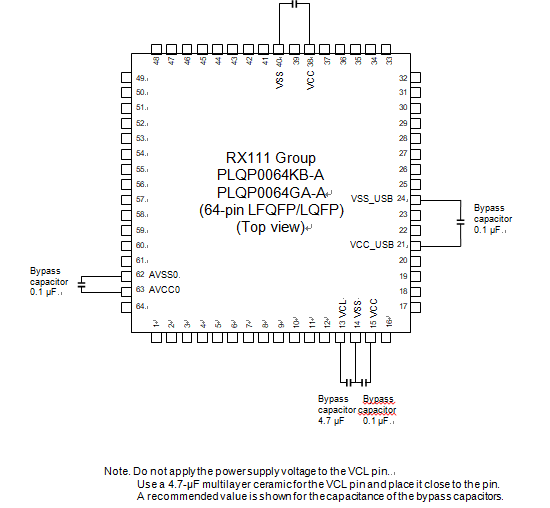
Use a 4.7-µF multilayer ceramic for the VCL pin and place it close to the pin. A recommended value is shown for the capacitance of the bypass capacitors
Use a recommended value of 0.1 μF as the capacitance of the capacitors. For the capacitors related to crystal oscillation, see section 9, Clock Generation Circuit in the User’s Manual: Hardware. For the capacitors related to analog modules, also see section 30, 12-Bit A/D Converter (S12ADb) in the User’s Manual: Hardware.
 Locked MCU ATMEGA32M1 Firmware Recovery
Locked MCU ATMEGA32M1 Firmware Recovery needs to unlock atmega32m1 microcontroller flash memory, then readout embedded software from atmega32m1 processor;
To drive the device from an external clock source, XTAL1 should be driven as shown in below Figure. To run the device on an external clock, the CKSEL Fuses must be programmed to “0000”. By programming the CKOPT Fuse, the user can enable an internal 36 pF capacitor between XTAL1 and GND, and XTAL2 and GND.
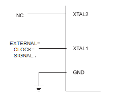
When applying an external clock, it is required to avoid sudden changes in the applied clock frequency to ensure stable operation of the MCU. A variation in frequency of more than 2% from one clock cycle to the next can lead to unpredictable behavior in the process of breaking atmega16l locked mcu flash memory. It is required to ensure that the MCU is kept in Reset during such changes in the clock frequency.
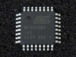
a recuperação de firmware MCU ATMEGA32M1 bloqueada precisa desbloquear a memória flash do microcontrolador atmega32m1 e, em seguida, ler o software incorporado do processador atmega32m1;
For AVR microcontrollers with Timer/Counter Oscillator pins (TOSC1 and TOSC2), the crystal is connected directly between the pins. By programming the CKOPT Fuse, the user can enable internal capacitors on XTAL1 and XTAL2 to recover microprocessor atmega16 protective flash, thereby removing the need for external capacitors. The Oscillator is optimized for use with a 32.768 kHz watch crystal. Applying an external clock source to TOSC1 is not recommended.
 Copy Locked R5F212DASNFP MCU Flash Data
Copy Locked R5F212DASNFP MCU Flash Data needs to crack RENESAS microcontroller fuse bit of flash memory, and then extract embedded firmware from microprocessor flash memory;
16 bits × 1 (with 4 capture/compare registers)
Timer mode (input capture function, output compare function), PWM mode (output 3 pins), PWM2 mode (PWM output pin)
16 bits × 2 (with 4 capture/compare registers)
Timer mode (input capture function, output compare function), PWM mode can be used for renesas locked mcu R5F212AASD memory data copying;
(output 6 pins), reset synchronous PWM mode (output three-phase waveforms (6 pins), sawtooth wave modulation), complementary PWM mode (output three-phase waveforms (6 pins), triangular wave modulation), PWM3 mode (PWM output 2 pins with fixed period)
8 bits × 1, Real-time clock mode (count seconds, minutes, hours, days of week), output compare mode
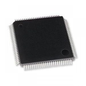
copiar dados de flash MCU R5F212DASNFP bloqueados precisa quebrar o microcontrolador RENESAS fundir bit de memória flash e, em seguida, extrair firmware incorporado da memória flash do microprocessador;
16 bits × 1 (with capture/compare register pin and compare register pin) Input capture mode, output compare mode to dump Renesas protected mcu r5f212a7sd flash program.
R8C/Tiny series core
- Number of fundamental instructions: 89
- Minimum instruction execution time:
50 ns (f(XIN) = 20 MHz, VCC = 3.0 to 5.5 V)
100 ns (f(XIN) = 10 MHz, VCC = 2.7 to 5.5 V)
200 ns (f(XIN) = 5 MHz, VCC = 2.2 to 5.5 V)
- Multiplier: 16 bits × 16 bits ® 32 bits
- Multiply-accumulate instruction: 16 bits × 16 bits + 32 bits ® 32 bits
Operation mode: Single-chip mode (address space: 1 Mbyte)
 Renesas Locked R5F212AASDFP Memory Data Copying
Renesas Locked R5F212AASDFP Memory Data Copying will need to decrypt renesas MCU R5F212AASDFP flash memory content, copy software to new microprocessor R5F212AASDFP;
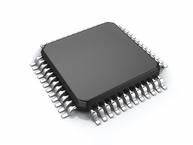
R0 is a 16-bit register for transfer, arithmetic, and logic operations. The same applies to R1 to R3. R0 can be split into high-order bits (R0H) and low-order bits (R0L) to be used separately as 8-bit data registers.
R1H and R1L are analogous to R0H and R0L. R2 can be combined with R0 and used as a 32-bit data register (R2R0). R3R1 is analogous to R2R0.
A0 is a 16-bit register for address register indirect addressing and address register relative addressing. It is also used for transfer, arithmetic, and logic operations. A1 is analogous to A0. A1 can be combined with A0 and as a 32- bit address register (A1A0).
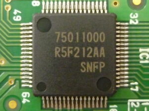
Renesas bloqueado R5F212AASDFP cópia de dados de memória precisará descriptografar renesas MCU R5F212AASDFP conteúdo de memória flash, copiar o software para o novo microprocessador R5F212AASDFP;
FB is a 16-bit register for FB relative addressing.
INTB is a 20-bit register that indicates the start address of an interrupt vector table.
 STM32F358RC Locked Microprocessor Flash Heximal Restoration
STM32F358RC Locked Microprocessor Flash Heximal Restoration firstly need to crack secured mcu stm32f358rc flash memory, then extract embedded firmware from encrypted microcontroller stm32f358rc flash memory;
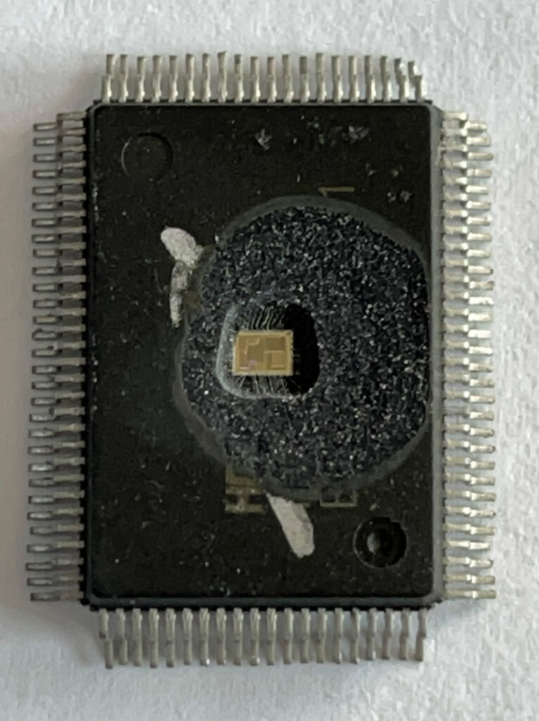
The ARM® Cortex®-M4 processor with FPU is the latest generation of ARM processors for embedded systems. It was developed to provide a low-cost platform that meets the needs of MCU implementation when recovering stm32f303zd embedded firmware from microcontroller flash memory, with a reduced pin count and low-power consumption, while delivering outstanding computational performance and an advanced response to interrupts.
The ARM® Cortex®-M4 32-bit RISC processor with FPU features exceptional code- efficiency, delivering the high-performance expected from an ARM core in the memory size usually associated with 8- and 16-bit devices. The processor supports a set of DSP instructions which allow efficient signal processing and complex algorithm execution to break stm32f302ve microprocessor flash memory.
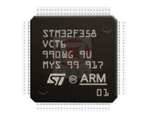
STM32F358RC bloqueado microprocessador flash restauração heximal primeiro precisa quebrar a memória flash mcu stm32f358rc segura, em seguida, extrair firmware incorporado do microcontrolador criptografado stm32f358rc memória flash
Its single precision FPU speeds up software development by using metalanguage development tools, while avoiding saturation. With its embedded ARM core, the STM32F358xC family is compatible with all ARM tools and software.
 STM32F303RE Microcontroller Flash Heximal Copying
STM32F303RE Microcontroller Flash Heximal Copying can help engineer to restore embedded firmware from locked mcu stm32f303re, and then dump heximal file to new microprocessor stm32f303re;

Each power supply pair (VDD/VSS, VDDA/VSSA etc.) must be decoupled with filtering ceramic capacitors as shown above. These capacitors must be placed as close as possible to break secured microcontroller stm32f302vd flash memory, or below the appropriate pins on the underside of the PCB to ensure the good functionality of the device.
Stresses above the absolute maximum ratings listed in Table 16: Voltage characteristics, Table 17: Current characteristics, and Table 18: Thermal characteristics may cause permanent damage to the device. These are stress ratings only and functional operation of the device at these conditions is not implied. Exposure to maximum rating conditions for extended periods may affect device reliability.
STM32F303RE microcontrolador flash cópia heximal pode ajudar o engenheiro para restaurar o firmware incorporado de bloqueado mcu stm32f303re e, em seguida, despejar arquivo heximal para o novo microprocessador stm32f303re;
All main power (VDD, VDDA) and ground (VSS, VSSA) pins must always be connected to the external power supply to break stm32f302zd microcontroller flash memory, in the permitted range. The following relationship must be respected between VDDA and VDD:
VDDA must power on before or at the same time as VDD in the power up sequence.
VDDA must be greater than or equal to VDD.
- VREF+ must be always lower or equal than VDDA (VREF+ £VDDA). If unused then it must be connected to VDDA.
VIN maximum must always be respected. Refer to Table 17: Current characteristics for the maximum allowed injected current values.
 Secured Microcontroller STM32F303ZD Embedded Firmware Recovery
Secured Microcontroller STM32F303ZD Embedded Firmware Recovery needs to unlock mcu stm32f303zd flash memory, and then readout heximal file from stm32f303zd microprocessor;
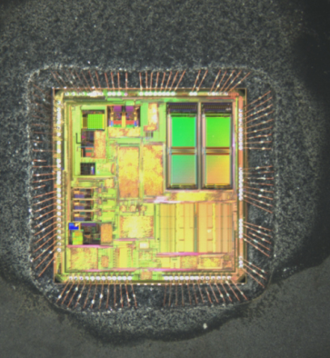
The STM32F303xD/E family is based on the high-performance ARM® Cortex®-M4 32-bit RISC core with FPU operating at a frequency of 72 MHz, and embedding a floating point unit (FPU), a memory protection unit (MPU) and an embedded trace macrocell (ETM).
The family incorporates high-speed embedded memories (512-Kbyte Flash memory, 80-Kbyte SRAM), a flexible memory controller (FSMC) for static memories when break stm32f301k6 microprocessor flash memory (SRAM, PSRAM, NOR and NAND), and an extensive range of enhanced I/Os and peripherals connected to an AHB and two APB buses.
The devices offer four fast 12-bit ADCs (5 Msps), seven comparators, four operational amplifiers, two DAC channels, a low-power RTC, up to five general-purpose 16-bit timers, one general-purpose 32-bit timer, and up,to three timers dedicated to motor control.
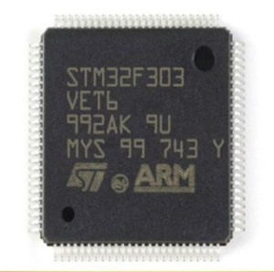
microcontrolador seguro STM32F303ZD recuperação de firmware incorporado precisa desbloquear mcu stm32f303zd memória flash e, em seguida, ler o arquivo heximal do microprocessador stm32f303zd
They also feature standard and advanced communication interfaces: up to three I2Cs, up to four SPIs (two SPIs are with multiplexed full-duplex I2Ss), three USARTs in the process of restoring stm32f301r8 secured mcu flash firmware, up to two UARTs, CAN and USB. To achieve audio class accuracy, the I2S peripherals can be clocked via an external PLL.
The STM32F303xD/E family operates in the -40 to +85°C and -40 to +105°C temperature ranges from a 2.0 to 3.6 V power supply. A comprehensive set of power-saving mode allows the design of low-power applications. The STM32F303xD/E family offers devices in different packages ranging from 64 to 144 pins.
 Encrypted Microcontroller STM32F302ZE Flash Data Recovery
Encrypted Microcontroller STM32F302ZE Flash Data Recovery will be able to completed embedded heximal extraction over secured mcu stm32f302ze, after cracking secured microprocessor stm32f302ze flash memory;
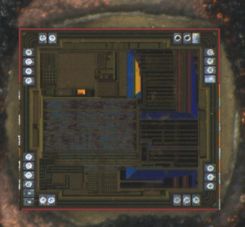
The STM32F302xD/E supports three low-power modes to achieve the best compromise between low power consumption, short startup time and available wakeup sources:
- Sleep mode
In Sleep mode, only the CPU is stopped. All peripherals continue to operate and wake up the CPU when an interrupt/event occurs.
- Stop mode
Stop mode achieves the lowest power consumption while retaining the content of SRAM and registers. All clocks in the 1.8 V domain are stopped, the PLL in the process of stm32f301r8 mcu flash firmware restoration, the HSI RC and the HSE crystal oscillators are disabled. The voltage regulator can also be put either in normal or in low-power mode.
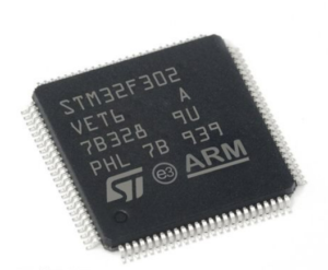
microcontrolador criptografado STM32F302ZE recuperação de dados flash será capaz de completar a extração heximal incorporada sobre seguro mcu stm32f302ze, depois de quebrar a memória flash segura do microprocessador stm32f302ze
The device can be woken up from Stop mode by any of the EXTI line. The EXTI line source can be one of the 16 external lines, the PVD output, the USB wakeup, the RTC alarm, COMPx, I2Cx or U(S)ARTx.
- Standby mode
The Standby mode is used to achieve the lowest power consumption. The internal voltage regulator is switched off so that the entire 1.8 V domain is powered off. The PLL, the HSI RC and the HSE crystal oscillators are also switched off to break encrypted stm32f301k6 microprocessor flash memory.
After entering Standby mode, SRAM and register contents are lost except for registers in the Backup domain and Standby circuitry. The device exits Standby mode when an external reset (NRST pin), an IWDG reset, a rising edge on the WKUP pin or an RTC alarm occurs.
 STM32F302RE Microprocessor Flash Heximal Restoration
STM32F302RE Microprocessor Flash Heximal Restoration needs to crack stm32f302re locked mcu fuse bit, and dump the embedded firmware content from stm32f302re microcontroller flash memory;
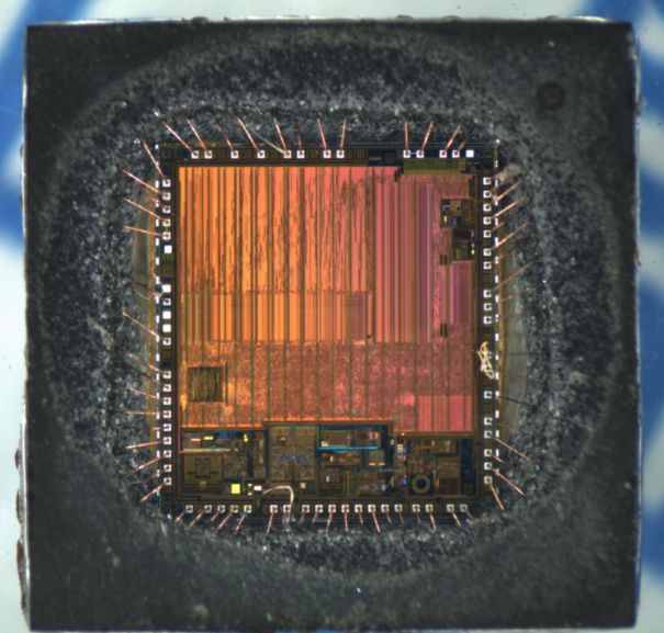
All STM32F302xD/E devices feature 384/512 Kbyte of embedded Flash memory available for storing programs and data. The Flash memory access time is adjusted to the CPU clock frequency (0 wait state from 0 to 24 MHz, 1 wait state from 24 to 48 MHz and 2 wait states above).
STM32F302xD/E devices feature 64 Kbyte of embedded SRAM with hardware parity check implemented on the first 32 Kbyte to attacking stm32f301k8 locked microcontroller readout protection. The memory can be accessed in read/write at CPU clock speed with 0 wait states.
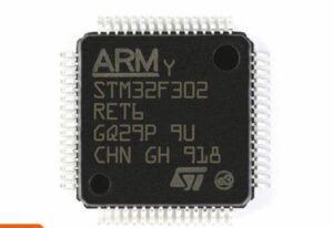
La restauración hexadal del flash del microprocesador STM32F302RE necesita descifrar el bit de fusible del MCU bloqueado STM32F302RE y volcar el contenido del firmware incorporado de la memoria flash del microcontrolador STM32F302RE;
At startup, Boot0 pin and Boot1 option bit are used to select one of three boot options:
- Boot from user Flash
- Boot from system memory
- Boot from embedded SRAM
The boot loader is located in the system memory. It is used to reprogram the Flash memory by using USART1 (PA9/PA10), USART2 (PA2/PA3) or USB (PA11/PA12) through DFU (device firmware upgrade).
The CRC (cyclic redundancy check) calculation unit is used to get a CRC code using a configurable generator polynomial value and size.
Among other applications, CRC-based techniques are used to verify data transmission or storage integrity. In the scope of the EN/IEC 60335-1 standard, they offer a means of verifying the Flash memory integrity.
 STM32F302RD Locked Microprocessor Flash Firmware Copying
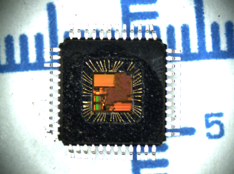
STM32F302RD Locked Microprocessor Flash Firmware Copying will need to disable the protection over stm32f302rd secured MCU through fuse bit by unlocking; and then extract heximal code from encrypted microcontroller stm32f302rd flash memory;
The STM32F302xD/E family is based on the high-performance ARM® Cortex®-M4 32-bit RISC core with FPU operating at a frequency of 72 MHz, and embedding a floating point unit (FPU), a memory protection unit (MPU) and an embedded trace macrocell (ETM).
The family incorporates high-speed embedded memories (512-Kbyte Flash memory, 64-Kbyte SRAM), a flexible memory controller (FSMC) for static memories (SRAM, PSRAM, NOR and NAND), and an extensive range of enhanced I/Os and peripherals connected to an AHB and two APB buses.
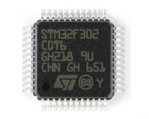
STM32F302RD заблокированный микропроцессор флэш-прошивки копирование прошивки потребует отключения защиты через защищенный микроконтроллер stm32f302rd через бит предохранителя путем разблокировки; а затем извлеките шестнадцатеричный код из зашифрованной флэш-памяти микроконтроллера Stm32f302rd
The devices offer two fast 12-bit ADCs (5 Msps), four comparators, two operational amplifiers, one DAC channel, a low-power RTC, up to two general-purpose 16-bit timers, one general-purpose 32-bit timer, and one timer dedicated to motor control.
They also feature standard and advanced communication interfaces: up to three I2Cs, up to four SPIs (two SPIs are with multiplexed full-duplex I2Ss), three USARTs, up to two UARTs, CAN and USB. To achieve audio class accuracy, the I2S peripherals can be clocked via an external PLL.