Archive for the ‘Recover MCU’ Category
 Dump Microcontroller ATMEGA128V Locked Code
We can dump microcontroller ATMEGA128V locked code, please view the microcontroller ATMEGA128V features for your reference:
The ATMEGA128V provides the following standard features: 12K bytes of Downloadable locked code, 256 bytes of RAM, 32 I/O lines, programmable watchdog timer, two Data Pointers, three 16-bit timer/counters, a six-vector two-level interrupt architecture, a full duplex serial port, on-chip oscillator, and clock circuitry.
In addition, the ATMEGA128V is designed with static logic for operation down to zero frequency and supports two software selectable power saving modes. The Idle Mode stops the CPU while allowing the RAM, timer/counters, serial port, and interrupt system to continue functioning if Dump Microcontroller ATMEGA128V Locked Code.
The Power Down Mode saves the RAM contents but freezes the oscillator, disabling all other chip functions until the next interrupt or hardware reset.
The Downloadable locked code can be changed a single byte at a time and is accessible through the SPI serial interface. Holding RESET active forces the SPI bus into a serial programming interface and allows the program memory to be written to or read from unless Lock Bit 2 has been activated after Dump Microcontroller ATMEGA128V Locked Code.
Port 0 is an 8-bit open drain bidirectional I/O port. As an output port, each pin can sink eight TTL inputs. When 1s are written to port 0 pins, the pins can be used as high impedance inputs. Port 0 can also be configured to be the multiplexed low order address/data bus during accesses to external program and data memory. In this mode, P0 has internal pullups.
Port 0 also receives the code bytes during locked code programming and outputs the code bytes during program verification. External pullups are required during program verification before Dump Microcontroller ATMEGA128V Locked Code.
Port 1 is an 8-bit bidirectional I/O port with internal pullups. The Port 1 output buffers can sink/source four TTL inputs. When 1s are written to Port 1 pins, they are pulled high by the internal pullups and can be used as inputs. As inputs, Port 1 pins that are externally being pulled low will source current (IIL) because of the internal pullups.
Some Port 1 pins provide additional functions. P1.0 and P1.1 can be configured to be the timer/counter 2 external count input (P1.0/T2) and the timer/counter 2 trigger input (P1.1/T2EX), respectively after REVERSE ENGINEERING MICROCONTROLLER.
 Recover Locked Chip ATMEGA128PV Binary
We can recover locked chip ATMEGA128PV binary, please view the locked chip ATMEGA128PV features for your reference:
Port 1 also receives the low-order address bytes during Flash programming and verification.
Port 2
Port 2 is an 8-bit bidirectional I/O port with internal pullups. The Port 2 output buffers can sink/source four TTL inputs. When 1s are written to Port 2 pins, they are pulled high by the internal pullups and can be used as inputs when Recover Locked Chip ATMEGA128PV Binary.
As inputs, Port 2 pins that are externally being pulled low will source current (IIL) because of the internal pullups. Port 2 emits the high-order address byte during fetches from external program memory and during accesses to external data memory that use 16-bit addresses (MOVX @ DPTR).
In this application, Port 2 uses strong internal pullups when emitting 1s. During accesses to external data memory that use 8-bit addresses (MOVX @ RI), Port 2 emits the contents of the P2 Special Function Register.
Port 2 also receives the high-order address bits and some control signals during Flash programming and verification.
Port 3
Port 3 is an 8 bit bidirectional I/O port with internal pullups. The Port 3 output buffers can sink/source four TTL inputs. When 1s are written to Port 3 pins, they are pulled high by the internal pullups and can be used as inputs after Recover Locked Chip ATMEGA128PV Binary.
As inputs, Port 3 pins that are externally being pulled low will source current (IIL) because of the pullups. Port 3 also serves the functions of various special features of the AT89S53, as shown in the following table. Port 3 also receives some control signals for Flash programming and verification.
Reset input. A high on this pin for two machine cycles while the oscillator is running resets the device.
ALE/PROG
Address Latch Enable is an output pulse for latching the low byte of the address during accesses to external memory. This pin is also the program pulse input (PROG) during Flash programming.
In normal operation, ALE is emitted at a constant rate of 1/6 the oscillator frequency and may be used for external timing or clocking purposes. Note, however, that one ALE pulse is skipped during each access to external data memory before RECOVER MCU.
 Decrypt Microprocessor ATMEGA169PA Code
We can decrypt Microprocessor ATMEGA169PA code, please view the Microprocessor ATMEGA169PA features for your reference:
SPI Registers Control and status bits for the Serial Peripheral Interface are contained in registers SPCR (shown in Table 4) and SPSR (shown in Table 5). The SPI data bits are contained in the SPDR register.
Writing the SPI data register during serial data transfer sets the Write Collision bit, WCOL, in the SPSR register. The SPDR is double buffered for writing and the values in SPDR are not changed by Reset if decrypt Microprocessor code.
Interrupt Registers The global interrupt enable bit and the individual interrupt enable bits are in the IE register. In addition, the individual interrupt enable bit for the SPI is in the SPCR register. Two priorities can be set for each of the six interrupt sources in the IP register before Decrypt Microprocessor ATMEGA169PA Code.
Dual Data Pointer Registers To facilitate accessing external data memory, two banks of 16 bit Data Pointer Registers are provided: DP0 at SFR address locations 82H-83H and DP1 at 84H-85H. Bit DPS = 0 in SFR WCON selects DP0 and DPS = 1 selects DP1.
The user should always initalize the DPS bit to the appropriate value before accessing the respective Data Pointer register.
Power Off Flag The Power Off Flag (POF) is located at bit_4 (PCON.4) in the PCON SFR. POF is set to “1” during power up. It can be set and reset under software control and is not affected by RESET when Decrypt Microprocessor ATMEGA169PA Code.
The ATMEGA169PA implements 256 bytes of RAM. The upper 128 bytes of RAM occupy a parallel space to the Special Function Registers. That means the upper 128 bytes have the same addresses as the SFR space but are physically separate from SFR space.
When an instruction accesses an internal location above address 7FH, the address mode used in the instruction specifies whether the CPU accesses the upper 128 bytes of RAM or the SFR space. Instructions that use direct addressing access SFR space.
For example, the following direct addressing instruction accesses the SFR at location 0A0H (which is P2) after Decrypt Microprocessor ATMEGA169PA Code.
 Reverse Engineering Microcomputer ATMEGA2560L Eeprom
We can reverse engineering Microcomputer ATMEGA2560L eeprom, please view the Microcomputer ATMEGA2560L features for your reference:
Timer 2 can be programmed to count up or down when configured in its 16 bit auto-reload mode. This feature is invoked by the DCEN (Down Counter Enable) bit located in the SFR T2MOD.
Upon reset, the DCEN bit is set to 0 so that timer 2 will default to count up. When DCEN is set, Timer 2 can count up or down, depending on the value of the T2EX pin if reverse engineering Microcomputer ATMEGA2560L eeprom.
Figure 2 shows Timer 2 automatically counting up when DCEN = 0. In this mode, two options are selected by bit EXEN2 in T2CON. If EXEN2 = 0, Timer 2 counts up to 0FFFFH and then sets the TF2 bit upon overflow.
The overflow also causes the timer registers to be reloaded with the 16 bit value in RCAP2H and RCAP2L. The values in RCAP2H and RCAP2L are preset by software. If EXEN2 = 1, a 16 bit reload can be triggered either by an overflow or by a 1-to-0 transition at external input T2EX after reverse engineering Microcomputer ATMEGA2560L eeprom.
This transition also sets the EXF2 bit. Both the TF2 and EXF2 bits can generate an interrupt if enabled. Setting the DCEN bit enables Timer 2 to count up or down, as shown in Figure 3. In this mode, the T2EX pin controls the direction of the count. A logic 1 at T2EX makes Timer 2 count up when reverse engineering Microcomputer eeprom.
The timer will overflow at 0FFFFH and set the TF2 bit. This overflow also causes the 16 bit value in RCAP2H and RCAP2L to be reloaded into the timer registers, TH2 and TL2, respectively if reverse engineering Microcomputer ATMEGA2560L eeprom.
A logic 0 at T2EX makes Timer 2 count down. The timer underflows when TH2 and TL2 equal the values stored in RCAP2H and RCAP2L. The underflow sets the TF2 bit and causes 0FFFFH to be reloaded into the timer registers.
The EXF2 bit toggles whenever Timer 2 overflows or underflows and can be used as a 17th bit of resolution. In this operating mode, EXF2 does not flag an interrupt.
 Reverse Engineering Chip ATMEGA640 Flash
We can reverse engineering chip ATMEGA640 flash, please view the chip ATMEGA640 features for your reference:
The interconnection between master and slave CPUs with SPI is shown in the following figure. The SCK pin is the clock output in the master mode but is the clock input in the slave mode when reverse engineering chip flash.
Writing to the SPI data register of the master CPU starts the SPI clock generator, and the data written shifts out of the MOSI pin and into the MOSI pin of the slave CPU. After shifting one byte, the SPI clock generator stops, setting the end of transmission flag (SPIF) if reverse engineering chip flash.
If both the SPI interrupt enable bit (SPIE) and the serial port interrupt enable bit (ES) are set, an interrupt is requested. The Slave Select input, SS/P1.4, is set low to select an individual SPI devchipe as a slave. When SS/P1.4 is set high, the SPI port is deactivated and the MOSI/P1.5 pin can be used as an input.
There are four combinations of SCK phase and polarity with respect to serial data, whchiph are determined by control bits CPHA and CPOL. The SPI data transfer formats.
The AT89S53 has a total of six interrupt vectors: two external interrupts (INT0 and INT1), three timer interrupts (Timers 0, 1, and 2), and the serial port interrupt when reverse engineering chip flash.
Each of these interrupt sources can be individually enabled or disabled by setting or clearing a bit in Special Function Register IE. IE also contains a global disable bit, EA, whchiph disables all interrupts at once.
Note that Table 10 shows that bit position IE.6 is unimplemented. In the AT89C51, bit position IE.5 is also unimplemented. User software should not write 1s to these bit positions, since they may be used in future AT89 products. Timer 2 interrupt is generated by the logchipal OR of bits TF2 and EXF2 in register T2CON before reverse engineering chip flash.
Neither of these flags is cleared by hardware when the servchipe routine is vectored
In fact, the servchipe routine may have to determine whether it was TF2 or EXF2 that generated the interrupt, and that bit will have to be cleared in software.
The Timer 0 and Timer 1 flags, TF0 and TF1, are set at S5P2 of the cycle in whchiph the timers overflow. The values are then polled by the circuitry in the next cycle. However, the Timer 2 flag, TF2, is set at S2P2 and is polled in the same cycle in whchiph the timer overflows after REVERSE ENGINEERING MICROCONTROLLER.
 Reverse Engineering Microcomputer ATmega2560 Program
Reverse Engineering Microcomputer ATmega2560 internal memory, and extract MCU ATmega2560 Program out from flash memory, crack Microcontroller ATmega2560 security fuse bit by focus ion beam technique;
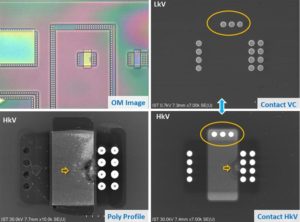
Reverse Engineering Microcomputer ATmega2560 internal memory, and extract MCU ATmega2560 Program out from flash memory, crack Microcontroller ATmega2560 security fuse bit by focus ion beam technique
If lock bits LB1 and LB2 have not been programmed, the programmed Code can be read back via the address and data lines for verification. The state of the lock bits can also be verified directly in the parallel programming mode when copying infineon saf-xc888cm-8ffi binary.
In the serial programming mode, the state of the lock bits can only be verified indirectly by observing that the lock bit features are enabled. In the parallel programming mode, Microcomputer erase is initiated by using the proper combination of control signals and by holding ALE/PROG low for 10 ms.
The Code array is written with all “1”s in the Microcomputer Erase operation. In the serial programming mode, a Microcomputer erase operation is initiated by issuing the Microcomputer Erase instruction. In this mode, Microcomputer erase is self-timed and takes about 16 ms.
During Microcomputer erase, a serial read from any address location will return 00H at the data outputs. A programmable fuse is available to disable Serial Programming if the user needs maximum system security after recover Microcomputer C8051F340 firmware.
The Serial Programming Fuse can only be programmed or erased in the Parallel Programming Mode. The AT89S53 is shipped with the Serial Programming Mode enabled.
Reading the Signature Bytes: The signature bytes are read by the same procedure as a normal verification of locations 030H and 031H, except that P3.6 and P3.7 must be pulled to a logic low. The values returned are as follows:
(030H) = 1EH indicates manufactured by Atmel
(031H) = 53H indicates 89S53
Every code byte in the program array can be written, and the entire array can be erased, by using the appropriate combination of control signals. The write operation cycle is self-timed and once initiated, will automatically time itself to completion.
All major programming vendors offer worldwide support for the Atmel microcontroller series. Please contact your local programming vendor for the appropriate software revision.
 Restore IC Program
Restore IC Program from its embedded flash memory and eeprom memory has to change the status of Microcontroller from encrypted to un-encrypted, then readout code from MCU memory with universal programmer;
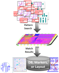
Restore IC Program from its embedded flash memory and eeprom memory has to change the status of Microcontroller from encrypted to un-encrypted, then readout code from MCU memory with universal programmer
Semiconductor manufacturers offer valuable customers an easy way to increase the protection of their products: IC chips with custom marking on the packages instead of standard chip names. That gives the impression that the final product was designed using ASICs or full custom ICs.
‘Everyone knows’ that ASICs offer very good protection against different sorts of ic attacks and only well equipped and highly skilled ic crackers could succeed with br restore IC program from them. This may stop many potential mcu attackers fiddling with the product.
However, a determined mcu cracker could try an easy way to check whether this chip was actually an ASIC. The easy way is to note which pins are connected to power supply, ground, clock, reset, serial, and other interfaces, and to compare all this information with the database of suspect microcontrollers or other ICs.
This works very reliably, as each microcontroller family has its own characteristic pinout. Once similarities are found the suspected microcontroller could be verified by placing it into a programming device or universal programmer and trying to read it.
 Decrypt Microprocessor ATmega2561 Dump
Decrypt Microprocessor ATmega2561 memory and extract dump from flash memory and eeprom memory, the content include program and data which will be presented in the format of binary or heximal;
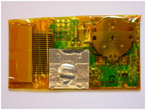
Decrypt Microprocessor ATmega2561 memory and extract dump from flash memory and eeprom memory, the content include program and data which will be presented in the format of binary or heximal
The ATmega2561 AVR is supported with a full suite of program and system development tools including: C compilers, macro assemblers, program debugger/simulators, in-circuit emulators, and evaluation kits. Each device in the ATmega2561 family differs only in memory size and number of pins. Table 1 summarizes the different configurations for the six devices.
Port A is an 8-bit bi-directional I/O port with internal pull-up resistors (selected for each bit). The Port A output buffers have symmetrical drive characteristics with both high sink and source capability before decrypt copy microcontroller P87C51X2BBD binary.
As inputs, Port A pins that are externally pulled low will source current if the pull-up resistors are activated. The Port A pins are tri-stated when a reset condition becomes active, even if the clock is not running. Port B is an 8-bit bi-directional I/O port with internal pull-up resistors (selected for each bit).
The Port B output buffers have symmetrical drive characteristics with both high sink and source capability. As inputs, Port B pins that are externally pulled low will source current if the pull-up resistors are activated when recovery Microprocessor AT89C4051 heximal.
The Port B pins are tri-stated when a reset condition becomes active, even if the clock is not running. Port B has better driving capabilities than the other ports.
Port C is an 8-bit bi-directional I/O port with internal pull-up resistors (selected for each bit). The Port C output buffers have symmetrical drive characteristics with both high sink and source capability. As inputs, Port C pins that are externally pulled low will source current if the pull-up resistors are activated. The Port C pins are tri-stated when a reset condition becomes active, even if the clock is not running.
Port D is an 8-bit bi-directional I/O port with internal pull-up resistors (selected for each bit). The Port D output buffers have symmetrical drive characteristics with both high sink and source capability.
As inputs, Port D pins that are externally pulled low will source current if the pull-up resistors are activated. The Port D pins are tri-stated when a reset condition becomes active, even if the clock is not running.
 Reverse Engineering MCU ATtiny48V Eeprom
Reverse Engineering MCU ATtiny48V Eeprom physical structure in the reverse order of microcontroller ATtiny48v manufacturing, security fuse bit can be located and crack microcontroller‘s bit, so the firmware can be readout from MCU memory;
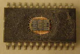
This section discusses the AVR core architecture in general. The main function of the CPU core is to ensure correct program execution. The CPU must therefore be able to access memories, perform calculations, control peripherals, and handle interrupts. In order to maximize performance and parallelism, the AVR uses a Harvard architecture – with separate memories and buses for program and data. Instructions in the program memory are executed with a single level pipelining.
While one instruction is being executed, the next instruction is pre-fetched from the program memory. This concept enables instructions to be executed in every clock cycle. The program memory is In System Reprogrammable eeprom memory. The fast-access Register File contains 32 x 8-bit general purpose working registers with a single clock cycle access time.
This allows single-cycle Arithmetic Logic Unit (ALU) operation.
In a typMCUal ALU operation, two operands are output from the Register File, the operation is executed, and the result is stored back in the Register File – in one clock cycle. Six of the 32 registers can be used as three 16-bit indirect address register pointers for Data Space addressing – enabling effMCUient address calculations.
One of the these address pointers can also be used as an address pointer for look up tables in eeprom program memory. These added function registers are the 16-bit X-, Y-, and Z-register, described later in this section.
The ALU supports arithmet and logic operations between registers or between a constant and a register. Single register operations can also be executed in the ALU. After an arithmetic operation, the Status Register is updated to reflect information about the result of the operation.
Program flow is provided by conditional and unconditional jump and call instructions, able to directly address the whole address space. Most AVR instructions have a single 16-bit word format. Every program memory address contains a 16- or 32-bit instruction after REVERSE ENGINEERING MICROCONTROLLER.
 Reverse Engineering MCU ATmega324PV Heximal
Reverse Engineering MCU ATmega324PV to extract microcontroller ATmega324PV scheme, locate the fuse bit and crack MCU’s memory for Heximal reading;
These options should only be used when not operating close to the maximum frequency of the device, and only if frequency stability at start-up is not important for the application. These options are not suitable for crystals.
These options are intended for use with ceramic resonators and will ensure frequency stability at start-up. They can also be used with crystals when not operating close to the maximum frequency of the device, and if frequency stability at start-up is not important for the application if copy chip at89s8252 flash.
The device can utilize a 32.768 kHz watch crystal as clock source by a dedicated Low Frequency Crystal Oscillator. The crystal should be connected as shown in Figure 22. When this Oscillator is selected, start-up times are determined by the SUT Fuses and CKSEL0.
The calibrated internal RC Oscillator by default provides a 8.0 MHz clock. The frequency is nominal value at 3V and 25°C. The device is shipped with the CKDIV8 Fuse programmed. See “System Clock Prescaler” on page 48 for more details. This clock may be selected as the system clock by programming the CKSEL Fuses as shown in Table.
If selected, it will operate with no external components. During reset, hardware loads the calibration byte into the OSCCAL Register and thereby automatically calibrates the RC Oscillator. At 3V and 25°C, this calibration gives a frequency of 8 MHz ± 1%.
The oscillator can be calibrated to any frequency in the range 7.3 – 8.1 MHz within ±1% accuracy, by changing the OSCCAL register. When this Oscillator is used as the MCU clock, the Watchdog Oscillator will still be used for the Watchdog Timer and for the Reset Time-out. For more information on the pre-programmed calibration value when Recover chip pic16f913 binary.
The device is shipped with this option selected.
The frequency ranges are preliminary values. Actual values are TBD.
If 8 MHz frequency exceeds the specification of the device (depends on VCC), the CKDIV8 Fuse can be programmed in order to divide the internal frequency by 8. When this Oscillator is selected, start-up times are determined by the SUT Fuses.
The Oscillator Calibration Register is used to trim the Calibrated Internal RC Oscillator to remove process variations from the oscillator frequency. The factory-calibrated value is automatically written to this register during MCU reset, giving an oscillator frequency of 8.0 MHz at 25°C.
The application software can write this register to change the oscillator frequency. The oscillator can be calibrated to any frequency in the range 7.3 – 8.1 MHz within ±1% accuracy. Calibration outside that range is not guaranteed.