Archive for the ‘Recover MCU’ Category
 Secured Microcontroller STM32F407ZG Embedded Firmware Restoration
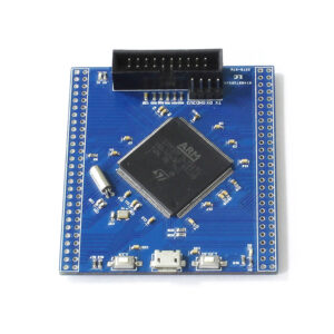
Unlock protective MCU STM32F407ZG Secured Microcontroller security fuse bit and extract program file include binary content of flash memory and eeprom data of rom memory from microprocessor STM32407ZG to fulfill STM32F407ZG Embedded Firmware Restoration;
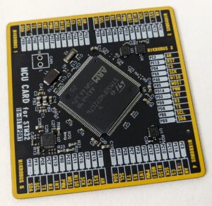
Unlock protective MCU STM32F407ZG Secured Microcontroller security fuse bit and extract program file include binary content of flash memory and eeprom data of rom memory from microprocessor STM32407ZG to fulfill STM32F407ZG Embedded Firmware Restoration;
The STM32F407ZG is a microcontroller unit (MCU) manufactured by STMicroelectronics. It belongs to the STM32F4 series, which is based on the ARM Cortex-M4 core and it becomes more difficult than other series to recover secured mcu stm32f405rg binary program. This MCU is highly versatile and can be used in various products across different industries. Here are some examples of products where the STM32F407ZG can be utilized:
Embedded Systems: The STM32F407ZG is commonly used in embedded systems for a wide range of applications such as industrial automation, robotics, home automation, and consumer electronics. Its powerful processing capabilities, extensive peripheral set, and low power consumption make it suitable for controlling and managing various functions within these systems.
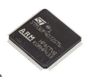
desbloquee la MCU protectora STM32F407ZG el bit de fusible de seguridad del microcontrolador seguro y extraiga el archivo de programa que incluye el contenido binario de la memoria flash y los datos de EEPROM de la memoria ROM del STM32407ZG del microprocesador para cumplir con STM32F407ZG restauración de firmware integrado;
Communications Equipment: The STM32F407ZG can be employed in communications equipment such as modems, routers, gateways, and network switches. Its high-speed processing capabilities and support for various communication protocols make it ideal for managing data transmission, networking, and connectivity tasks.
Medical Devices: In the medical industry, the STM32F407ZG can be used in devices such as patient monitors, medical imaging systems, infusion pumps, and diagnostic equipment. Its reliability, real-time processing capabilities, and support for safety-critical applications make it well-suited for use in medical devices that require precise control and monitoring.
Automotive Electronics: Automotive applications for the STM32F407ZG include engine control units (ECUs), dashboard displays, infotainment systems, advanced driver assistance systems (ADAS), and vehicle telematics. Its high performance, automotive-grade reliability, and support for automotive communication protocols make it suitable for use in various automotive electronics applications.
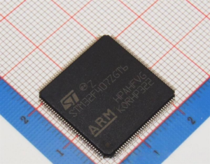
отключване на защитен MCU STM32F407ZG защитен микроконтролер сигурност предпазител бит и извличане на програмен файл включва двоично съдържание на флаш памет и eeprom данни на ROM памет от микропроцесорни STM32407ZG за изпълнение STM32F407ZG вграден фърмуер възстановяване;
Consumer Electronics: The STM32F407ZG can be found in consumer electronics products such as smart home devices, wearable gadgets, gaming consoles, multimedia players, and digital cameras. Its processing power, low power consumption, and support for multimedia interfaces make it attractive for implementing advanced features and functionalities in these products.
Industrial Control Systems: Industrial control systems, including programmable logic controllers (PLCs), supervisory control and data acquisition (SCADA) systems, and process automation equipment, often utilize the STM32F407ZG for monitoring and controlling industrial processes. Its robustness, real-time processing capabilities, and support for industrial communication protocols make it suitable for use in industrial environments.
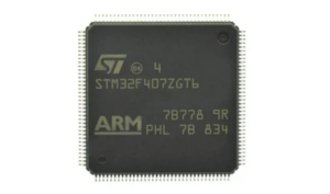
koruyucu MCU’nun kilidini açın STM32F407ZG güvenli mikrodenetleyici güvenlik sigorta biti ve program dosyasını çıkarın, gömülü STM32F407ZG ürün yazılımı geri yüklemesini yerine getirmek için mikroişlemci STM32407ZG’den flash belleğin ikili içeriğini ve rom belleğinin eeprom verilerini dahil edin;
Overall, the STM32F407ZG is a versatile microcontroller that can be employed in a wide range of products across multiple industries, thanks to its powerful features, extensive peripheral set, and flexibility for various applications.
 Decode encrypted STM32F405ZG microcontroller flash program
Decode encrypted STM32F405ZG microcontroller flash program starts from attack locked MCU STM32F405ZG tamper resistance system and readout embedded firmware from microprocessor STM32F405ZG flash memory as a binary code or heximal data;
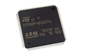
Decode encrypted STM32F405ZG microcontroller flash program starts from attack locked MCU STM32F405ZG tamper resistance system and readout embedded firmware from microprocessor STM32F405ZG flash memory as a binary code or heximal data;
Manufacturing an STM32F405 microcontroller involves several steps and processes. Here’s a general overview:
Design Phase: This involves designing the STM32F405 microcontroller, which includes the architecture, circuitry, and functionalities. STMicroelectronics, the manufacturer of STM32 microcontrollers, typically handles this phase.
Silicon Wafer Production: The microcontroller’s design is etched onto a silicon wafer using lithography techniques. This process is highly complex and involves creating multiple layers of the integrated circuit.
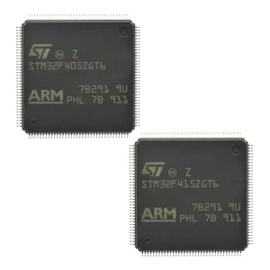
decodificar STM32F405ZG programa flash de microcontrolador encriptado comienza desde el sistema de resistencia a la manipulación de la MCU STM32F405ZG bloqueado por ataque y lectura del firmware integrado del microprocesador STM32F405ZG la memoria flash como código binario o datos hexaimales;
Wafer Testing: After the silicon wafer is processed, it undergoes testing to ensure that the individual microcontrollers on the wafer meet quality standards. Defective units are marked for later disposal.
Die Separation: The wafer is cut into individual dies, each containing a single STM32F405 microcontroller.
Packaging: Each die is then packaged into a protective housing, which provides electrical connections and protection from environmental factors.
Testing: The packaged microcontrollers undergo rigorous testing to ensure functionality and quality. This includes both electrical and functional tests.
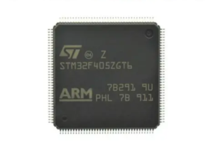
декодиране криптиран STM32F405ZG микроконтролер флаш програма започва от атака заключена MCU STM32F405ZG система за устойчивост на подправяне и четене вграден фърмуер от микропроцесор STM32F405ZG флаш памет като двоичен код или heximal данни;
Programming: The microcontrollers are programmed with the firmware necessary to operate them and copy locked microprocessor stm32f405zg memory heximal file. This firmware typically includes the STM32F405’s initial bootloader and any other necessary software.
Quality Control: Throughout the manufacturing process, quality control measures are implemented to ensure that the finished products meet specifications and standards.
Distribution: Once the microcontrollers pass all quality checks, they are ready for distribution to customers, typically electronic device manufacturers who will integrate them into their products.
It’s important to note that manufacturing microcontrollers like the STM32F405 involves highly specialized equipment and expertise, and is typically carried out by semiconductor fabrication facilities (fabs) with significant investment and infrastructure.

şifreli STM32F405ZG mikrodenetleyici flash programının kodunu çözmek, saldırı kilitli MCU’dan STM32F405ZG kurcalamaya karşı direnç sisteminden başlar ve mikroişlemci STM32F405ZG flash bellekten gömülü bellenimi ikili kod veya onaltılık veri olarak okur;
Unless you have the resources and expertise to set up such a facility, manufacturing STM32F405 microcontrollers would not be feasible on an individual or small scale. Instead, you would typically purchase these microcontrollers from authorized distributors or directly from STMicroelectronics.
 Protective STM32F405VG Microprocessor Content Restoration
Protective STM32F405VG Microprocessor Content Restoration is a process to unlock the secured microcontroller STM32F405VG readout-protection system and copy embedded firmware from STM32F405VG flash memory in the format of binary or heximal;
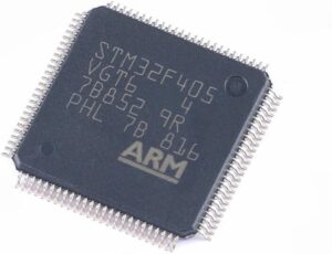
Protective STM32F405VG Microprocessor Content Restoration is a process to unlock the secured microcontroller STM32F405VG readout-protection system and copy embedded firmware from STM32F405VG flash memory in the format of binary or heximal;
The internal structure of the STM32F405VG microcontroller from STMicroelectronics is complex and includes several key components that enable its functionality. Here’s an overview of the internal structure:
ARM Cortex-M4 Core: The STM32F405VG is built around the ARM Cortex-M4 core, which serves as the central processing unit (CPU). The Cortex-M4 core is a high-performance 32-bit RISC processor designed for embedded applications. It features a Harvard architecture with separate instruction and data buses, a pipelined architecture, and supports a wide range of instructions and addressing modes.
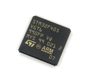
보호 STM32F405VG 마이크로프로세서 콘텐츠 복원은 보안 마이크로컨트롤러 STM32F405VG 판독 보호 시스템의 잠금을 해제하고 보안 MCU STM32F405VG 플래시 메모리에서 임베디드 펌웨어를 바이너리 또는 16진수 형식으로 복사하는 프로세스입니다.
Memory: The microcontroller typically includes various types of memory:
Flash Memory: This is used for storing the firmware (program code) of the microcontroller. The STM32F405VG typically comes with up to 1 MB of Flash memory.
SRAM (Static Random Access Memory): SRAM is used for storing data and variables during program execution. The STM32F405VG typically includes 192 KB of SRAM.
Registers: Registers are small, high-speed memory locations within the CPU used for temporary data storage and for holding control and status information.
Peripherals: The STM32F405VG incorporates a wide range of peripherals, including but not limited to:
USART, SPI, I2C interfaces for serial communication.
ADC (Analog-to-Digital Converter) and DAC (Digital-to-Analog Converter) channels for analog signal processing.
CAN (Controller Area Network) interfaces for automotive and industrial applications.
USB (Universal Serial Bus) interface for connectivity with external devices.
Timers, PWM (Pulse Width Modulation) channels, and GPIO (General-Purpose Input/Output) pins for various timing and control functions.
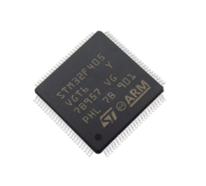
Phục hồi nội dung bảo vệ STM32F405VG vi xử lý là một quá trình để mở khóa vi điều khiển bảo mật STM32F405VG hệ thống bảo vệ đọc và sao chép phần sụn nhúng từ bộ nhớ MCU STM32F405VG flash được bảo mật ở định dạng nhị phân hoặc heximal;
DMA (Direct Memory Access) controller for efficient data transfer between peripherals and memory without CPU intervention.
Clock and Reset Management: The microcontroller includes a clock management unit responsible for generating and distributing clock signals to different parts of the device. It also includes a reset controller that manages the reset signals and initializes the device during power-up.
Power Management: Power management features are integrated into the microcontroller to regulate power consumption and optimize energy efficiency. This includes various low-power modes and features such as voltage scaling to adjust the operating voltage based on performance requirements.
Bus Matrix: The bus matrix is responsible for managing the data flow between the different components of the microcontroller, ensuring efficient communication and access to resources.
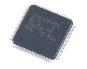
सुरक्षात्मक STM32F405VG माइक्रोप्रोसेसर सामग्री बहाली रीडआउट-प्रोटेक्शन सिस्टम STM32F405VG सुरक्षित माइक्रोकंट्रोलर को अनलॉक करने और सुरक्षित एमसीयू STM32F405VG फ्लैश मेमोरी से बाइनरी या हेक्सिमल के प्रारूप में एम्बेडेड फर्मवेयर कॉपी करने की एक प्रक्रिया है;
Debug and Trace Unit: The microcontroller includes a debug and trace unit that facilitates software debugging and system analysis by providing features such as breakpoint control, watchpoints, and real-time tracing of program execution.
Overall, the internal structure of the STM32F405VG is designed to provide a balance of performance, flexibility, and power efficiency, making it suitable for a wide range of embedded applications.
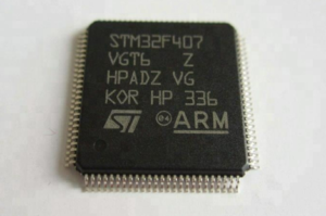
 Copy Locked Microprocessor STM32F407VG Memory Heximal
Copy locked Microprocessor STM32F407VG Memory Heximal can starts from unlock readout-protection mechanism of microcontroller STM32F407VG flash memory and extract embedded firmware of source code from STM32F407VG MCU flash and eeprom memory;
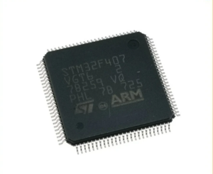
copy locked microprocessor STM32F407VG memory heximal can starts from unlock readout-protection mechanism of microcontroller STM32F407VG flash memory and extract embedded firmware of source code from STM32F407VG MCU flash and eeprom memory;
The STM32F405 finds application across diverse domains, thanks to its versatility and robust performance. Some notable applications include:
Industrial Automation: In industrial automation systems, the STM32F405 facilitates precise control of machinery and processes through its real-time processing capabilities and support for communication protocols such as Modbus, CAN, and Ethernet. From motor control to human-machine interface (HMI) applications, the STM32F405 enables efficient and reliable automation solutions.
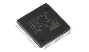
copiar bloqueado microprocessador STM32F407VG memória heximal pode começar a partir de desbloquear mecanismo de proteção de leitura de microcontrolador STM32F407VG memória flash e extrair firmware incorporado do código-fonte de STM32F407VG memória flash MCU e eeprom;
Consumer Electronics: In consumer electronics devices ranging from smart home appliances to portable gadgets, the STM32F405 powers innovative features such as touchscreens, wireless connectivity, and multimedia playback. Its low-power modes and efficient processing ensure optimal performance and extended battery life, enhancing the user experience.
Internet of Things (IoT): With built-in support for connectivity standards like Ethernet, Wi-Fi, and Bluetooth, the STM32F405 serves as a cornerstone for IoT devices and edge computing applications. Whether it’s collecting sensor data, transmitting telemetry to the cloud, or orchestrating local processing tasks, the STM32F405 offers the performance and connectivity required for IoT deployments.
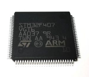
копіювання заблокованого мікропроцесора STM32F407VG шістнадцяткової пам’яті може запускатися з розблокування механізму захисту від зчитування мікроконтролера STM32F407VG флеш-пам’яті та вилучення вбудованої прошивки вихідного коду з STM32F407VG флеш-пам’яті MCU та EEPROM;
The STM32F405 microcontroller epitomizes the convergence of performance, versatility, and efficiency in embedded systems design. With its powerful ARM Cortex-M4 core, rich peripheral set, and integrated features, it empowers developers to realize their creative visions and tackle diverse challenges across industries.
کپی قفل شده میکروپروسسور STM32F407VG حافظه هگزیمال می تواند از مکانیسم باز کردن قفل حفاظت از میکروکنترلر STM32F407VG حافظه فلش شروع می شود و استخراج سیستم عامل تعبیه شده از کد منبع از STM32F407VG فلش MCU و حافظه eeprom؛
Whether it’s driving industrial automation, powering consumer electronics, or enabling the IoT revolution, the STM32F405 stands as a testament to the enduring impact of innovation in embedded technology. As the demand for smarter, more connected devices continues to grow, the STM32F405 remains a steadfast ally for developers pushing the boundaries of what’s possible in the world of embedded systems.
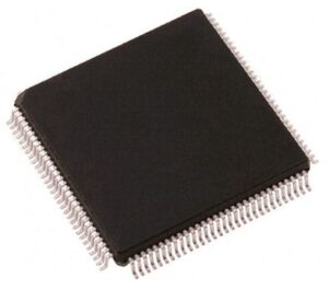
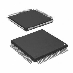
 Readout Renesas R7F7010124AFP Locked MCU Flash Content
Readout Renesas R7F7010124AFP Locked MCU Flash Content needs to firstly crack R7F7010124AFP secured microcontroller fuse bit and then copy flash program in the format of binary to new microprocessor R7F7010124afp;
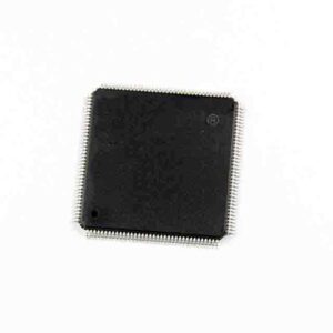
Readout Renesas R7F7010124AFP Locked MCU Flash Content needs to firstly crack R7F7010124AFP secured microcontroller fuse bit and then copy flash program in the format of binary to new microprocessor R7F7010124afp;
A strong electric field, when exposed to a MOS device, can cause destruction of the gate oxide and ultimately degrade the device operation. Steps must be taken to stop generation of static electricity as much as possible, and quickly dissipate it when it has occurred. Environmental control must be adequate.
When it is dry, a humidifier should be used. It is recommended to avoid using insulators that easily build up static electricity. Semiconductor devices must be stored and transported in an anti-static container when copying renesas microcontroller M306NKFH flash program, static shielding bag or conductive material. All test and measurement tools including work benches and floors should be grounded.
kiolvasás A RENESAS védő R7F7010124AFP zárolt MCU flash tartalomnak először fel kell törnie R7F7010124AFP biztonságos mikrovezérlő biztosítékbitjét, majd bináris forráskód vagy hexaximális adatok formájában flash programot kell másolnia az új mikroprocesszorra R7F7010124AFP
The operator should be grounded using a wrist strap. Semiconductor devices must not be touched with bare hands. Similar precautions need to be taken for PW boards with mounted semiconductor devices.
Power-on does not necessarily define the initial status of a MOS device. Immediately after the power source is turned ON, devices with reset functions have not yet been initialized when reading renesas microprocessor R5F212AASD flash binary file. Hence, power-on does not guarantee output pin levels, I/O settings or contents of registers. A device is not initialized until the reset signal is received. A reset operation must be executed immediately after power-on for devices with reset functions.
зчитування захисного R7F7010124AFP заблокованого вмісту мікроконтролера потрібно спочатку зламати R7F7010124AFP захищений біт запобіжника мікроконтролера, а потім скопіювати програму флеш-пам’яті у форматі двійкового вихідного коду або шістнадцяткових даних на новий мікропроцесор R7F7010124AFP
 Fujitsu Secured MCU MB90F345CAPF-G Heximal Code Restoration
Fujitsu Secured MCU MB90F345CAPF-G Heximal Code Restoration starts from attacking IC processor MB90F345 protection and readout microprocessor MB90F345 flash memory program;
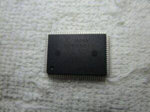
Fujitsu Secured MCU MB90F345CAPF-G Heximal Code Restoration starts from attacking IC processor MB90F345 protection and readout microprocessor MB90F345 flash memory program;
CMOS IC chips may suffer latch-up under the following conditions:
A voltage higher than VCC or lower than VSS is applied to an input or output
A voltage higher than the rated voltage is applied between VCC and VSS
The AVCC power supply is applied before the VCC
Latch-up may increase the power supply current drastically, causing thermal damage to the device.
For the same reason, also be careful not to let the analog power-supply voltage (AVCC, AVRH) exceed the digital power-supply voltage.
Leaving unused input pins open may result in misbehavior or latch-up and possible permanent damage to the device. Therefore they must be pulled up or pulled down through resistors. In this case those resistors should be more than 2 kL .
Unused bidirectional pins should be set to the output state and can be left open, or the input state with the above described connection.
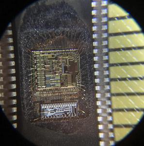
Restaurarea codului sursă binar sau heximal al MCU securizat FUJITSU MB90F345CAPF-G pornește de la microprocesorul de protecție împotriva fisurilor MB90F345 bit de siguranță și citirea blocată a microcontrolerului MB90F345 firmware încorporat din memoria flash
If there are multiple VCC and VSS pins, that are designed to be set to the same potential are connected the inside of the device to prevent malfunctions such as latch-up.
To reduce unnecessary radiation, prevent malfunctioning of the strobe signal due to the rise of ground level, and observe the standard for total output current, be sure to connect the VCC and VSS pins to the power supply and ground externally. Connect VCC and VSS pins to the device from the current supply source at a low impedance.
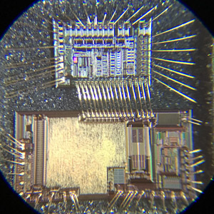
MCU protetto MB90F345CAPF-G il ripristino del codice sorgente binario o esadecimale inizia dal microprocessore protettivo contro le crepe Bit del fusibile di protezione MB90F345 e lettura bloccata Microcontroller MB90F345 firmware incorporato dalla sua memoria flash
Connect the mode pins directly to VCC or VSS pins. To prevent the device unintentionally entering test mode due to noise, lay out the printed circuit board so as to minimize the distance from the mode pins to VCC or VSS pins and to provide a low-impedance connection.
 Recover Secured MCU ATmega8U2 Flash Heximal
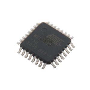
Recover Secured MCU ATmega8U2 Flash Heximal after unlock atmega8 microcontroller flash memory protection and extract avr chip atmega8u2 binary code from its flash and eeprom memory;
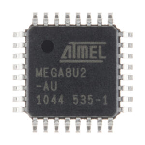
Recover Secured MCU ATmega8U2 Flash Heximal after unlock atmega8 microcontroller flash memory protection and extract avr chip atmega8u2 binary code from its flash and eeprom memory
The Power-down mode saves the register contents but freezes the Oscillator, disabling all other chip functions until the next interrupt or Hardware Reset. In Standby mode, the Crystal/Resonator Oscillator is running while the rest of the device is sleeping when pulling flash content of microchip atmega8u2 mcu memory. This allows very fast start-up combined with low power consumption. In Extended Standby mode, the main Oscillator continues to run.
The device is manufactured using Atmel’s high-density nonvolatile memory technology. The on- chip ISP Flash allows the program memory to be reprogrammed in-system through an SPI serial interface, by a conventional nonvolatile memory programmer, or by an on-chip Boot program running on the AVR core. The boot program can use any interface to download the application program in the application Flash memory when restoring atmega8l microcomputer flash data. Software in the Boot Flash section will continue to run while the Application Flash section is updated, providing true Read-While-Write operation. By combining an 8-bit RISC CPU with In-System Self-Programmable Flash on a monolithic chip, the Atmel ATmega8U2/16U2/32U2 is a powerful microcontroller that provides a highly flexible and cost effective solution to many embedded control applications.
 Recover Secured MCU PIC24FJ32GP202 Flash Program
Recover Secured MCU PIC24FJ32GP202 Flash Program from its memory needs to crack microcontroller pic24fj32gp202 flash memory and extract source code from pic24fj32gp202 microprocessor flash memory;
Recover Secured MCU PIC24FJ32GP202 Flash Program from its memory needs to crack microcontroller pic24fj32gp202 flash memory and extract source code from pic24fj32gp202 microprocessor flash memory
During programming and debugging, the resistance and capacitance that can be added to the pin must be considered. Device programmers and debuggers drive the MCLR pin. Consequently, specific voltage levels (VIH and VIL) and fast signal transitions must not be adversely affected. Therefore, specific values of R1 and C1 will need to be adjusted based on the application and PCB requirements.
For example, it is recommended that the capacitor, C1, be isolated from the MCLR pin during programming and debugging operations by using a jumper when executing microcontroller pic24fj16ga002 software decryption. The jumper is replaced for normal run-time operations. Any components associated with the MCLR pin should be placed within 0.25 inch (6 mm) of the pin.
- R1 ≤ 10 kΩ is A suggested starting value is 10 kΩ. Ensure that the MCLR pin VIH and VIL specifications are met.
- R2 ≤ 470Ω will limit any current flowing into MCLR from the external capacitor, C, in the event of a MCLR pin breakdown, due to Electrostatic Discharge (ESD) or Electrical Overstress (EOS). Ensure that the MCLR pin VIH and VIL specifications are met;
A low-ESR (< 5Ω) capacitor is required on the VCAP pin to stabilize the voltage regulator output voltage. The VCAP pin must not be connected to VDD and must use a capacitor of 10 µF connected to ground to break microcontroller pic24fj16ga002 flash memory heximal program. The type can be ceramic or tantalum. Suitable examples of capacitors are shown in Table 2-1. Capacitors with equivalent specifications can be used.
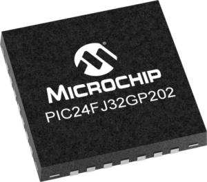
crack secured microcontroller PIC24FJ32GP202 and readout mcu chip PIC24FJ32GP202 flash memory program and eeprom memory data
Designers may use Figure 2-3 to evaluate the ESR equivalence of candidate devices. The placement of this capacitor should be close to VCAP. It is recommended that the trace length not exceed 0.25 inch (6 mm). Refer to 27.4 On-Chip Voltage Regulator for additional information.
 Locked STM32F207VET6 Microcontroller Firmware Code Restoration
Locked STM32F207VET6 Microcontroller Firmware Code Restoration is a process to crack protective stm32f207ve mcu flash memory then copy stm32f207vet6 mcu flash content to new microprocessor;
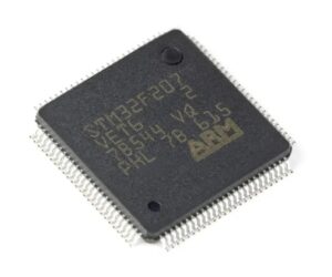
Locked STM32F207VET6 Microcontroller Firmware Code Restoration is a process to crack protective stm32f207ve mcu flash memory then copy stm32f207vet6 mcu flash content to new microprocessor;
These timers are based on a 16-bit auto-reload upcounter and a 16-bit prescaler. TIM10 and TIM11 feature one independent channel, whereas TIM9 has two independent channels for input capture/output compare, PWM or one-pulse mode output. They can be synchronized with the TIM2, TIM3, TIM4, TIM5 full-featured general-purpose timers. They can also be used as simple time bases.
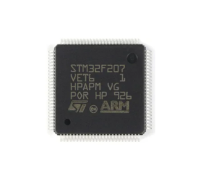
Zaključana STM32F207VET6 mikrokontrolera Ugrađena obnova firmware koda postupak je za razbijanje zaštitne STM32F207VET6 MCU flash memorije, a zatim izdvajanje STM32F207VET6 šifriranog mikroprocesorskog flash sadržaja u formatu binarne datoteke ili heksimalnih podataka u novi mikroprocesor
These timers are based on a 16-bit auto-reload upcounter and a 16-bit prescaler. TIM13 and TIM14 feature one independent channel, whereas TIM12 has two independent channels for input capture/output compare to recover stm32f205rc microcontroller’s flash memory heximal, PWM or one-pulse mode output. They can be synchronized with the TIM2, TIM3, TIM4, TIM5 full-featured general-purpose timers.
They can also be used as simple time bases.
These timers are mainly used for DAC trigger and waveform generation. They can also be used as a generic 16-bit time base.
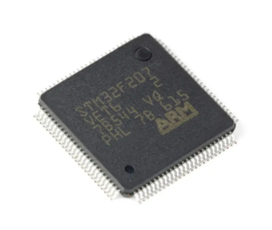
Przywracanie kodu oprogramowania układowego wbudowanego w mikrokontroler z zablokowanym STM32F207VET6 to proces polegający na złamaniu pamięci flash STM32F207VET6 ochronnej MCU, a następnie wyodrębnieniu STM32F207VET6 zaszyfrowanej zawartości flash mikroprocesora w formacie pliku binarnego lub danych szesnastkowych do nowego mikroprocesora
The independent watchdog is based on a 12-bit downcounter and 8-bit prescaler. It is clocked from an independent 32 kHz internal RC and as it operates independently from the main clock, it can operate in Stop and Standby modes. It can be used either as a watchdog to reset the device when a problem occurs, or as a free-running timer for application timeout.
 ARM Microcontroller STM32F205RG Flash Code Recovery
ARM Microcontroller STM32F205RG Flash Code Recovery starts from crack mcu chip stm32f205rg protective system and then decode secured flash memory software from microprocessor stm32f205rg;
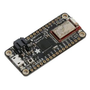
ARM Microcontroller STM32F205RG Flash Code Recovery starts from crack mcu chip stm32f205rg protective system and then decode secured flash memory software from microprocessor stm32f205rg;
The memory protection unit (MPU) is used to manage the CPU accesses to memory to prevent one task to accidentally corrupt the memory or resources used by any other active task. This memory area is organized into up to 8 protected areas that can in turn be divided up into 8 subareas. The protection area sizes are between 32 bytes and the whole 4 gigabytes of addressable memory.
La recuperación del código flash del microcontrolador ARM STM32F205RG comienza desde el sistema de protección crack mcu chip stm32f205rg y luego decodifica el software de memoria flash seguro del microprocesador stm32f205rg
The MPU is especially helpful for applications where some critical or certified code has to be protected against the misbehavior of other tasks. It is usually managed by an RTOS (real- time operating system). If a program accesses a memory location that is prohibited by the MPU, the RTOS can detect it and take action. In an RTOS environment, the kernel can dynamically update the MPU area setting, based on the process to be executed.
The MPU is optional and can be bypassed for applications that do not need it. The STM32F20x devices embed a 128-bit wide Flash memory of 128 Kbytes, 256 Kbytes, 512 Kbytes, 768 Kbytes or 1 Mbyte available for storing programs and data. The devices also feature 512 bytes of OTP memory that can be used to store critical user data such as Ethernet MAC addresses or cryptographic keys.
