Archive for the ‘Recover Chip’ Category
 Recover MCU PIC12CR509A Flash
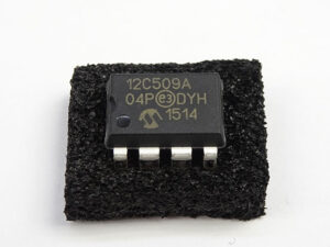
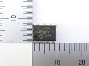
the PIC12CR509A microcontroller is widely used for its efficiency and compact design. However, many of these MCUs come with secured or locked firmware, making it challenging to access their flash memory or EEPROM data. This is where professional MCU crack services come into play, offering solutions to recover, decrypt, and extract critical information from protected chips.
Le microcontrôleur PIC12CR509A est largement utilisé pour son efficacité et sa conception compacte. Cependant, bon nombre de ces microcontrôleurs sont livrés avec un micrologiciel sécurisé ou verrouillé, ce qui rend difficile l’accès à leur mémoire flash ou à leurs données EEPROM. C’est là qu’interviennent les services professionnels de crackage de microcontrôleurs, proposant des solutions pour récupérer, décrypter et extraire des informations critiques à partir de puces protégées.
Using advanced techniques such as reverse engineering and binary analysis, experts can unlock the encrypted firmware of the PIC12CR509A. Whether the goal is to decode the source code, dump the flash memory, or replicate the program for further development, these services provide a pathway to bypass the secured barriers. By employing non-invasive methods, the original chip remains intact while the protected data is extracted.
역엔지니어링 및 바이너리 분석과 같은 고급 기술을 사용하여 전문가는 PIC12CR509A의 암호화된 펌웨어를 잠금 해제할 수 있습니다. 소스 코드를 디코딩하거나, 플래시 메모리를 덤프하거나, 추가 개발을 위해 프로그램을 복제하는 것이 목표이든, 이러한 서비스는 보안 장벽을 우회하는 경로를 제공합니다. 비침습적 방법을 사용함으로써 보호된 데이터가 추출되는 동안 원래 칩은 그대로 유지됩니다.
For those looking to hack or break into a locked MCU, specialized tools and software are used to attack the encryption algorithms. This process often involves decoding the binary files, analyzing the memory structure, and reconstructing the original firmware archive. Such services are invaluable for recovering lost data, cloning microcontrollers, or understanding the functionality of a protected microprocessor.
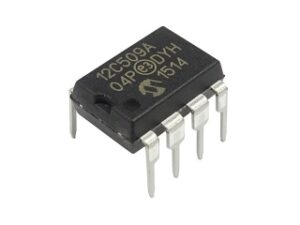
लॉक किए गए MCU को हैक करने या उसमें सेंध लगाने की चाहत रखने वालों के लिए, एन्क्रिप्शन एल्गोरिदम पर हमला करने के लिए विशेष उपकरण और सॉफ़्टवेयर का उपयोग किया जाता है। इस प्रक्रिया में अक्सर बाइनरी फ़ाइलों को डिकोड करना, मेमोरी संरचना का विश्लेषण करना और मूल फ़र्मवेयर संग्रह का पुनर्निर्माण करना शामिल होता है। ऐसी सेवाएँ खोए हुए डेटा को पुनर्प्राप्त करने, माइक्रोकंट्रोलर को क्लोन करने या संरक्षित माइक्रोप्रोसेसर की कार्यक्षमता को समझने के लिए अमूल्य हैं।
However, it’s important to note that MCU crack services should only be used for legitimate purposes, such as recovering data from a damaged chip or reverse engineering for compatibility improvements. With the right expertise, even the most secured PIC12CR509A flash memory can be unlocked, providing access to its hidden treasures.
We can Recover MCU PIC12CR509A Flash, please view the MCU PIC12CR509A features for your reference:
The PICCR509A each have 16 bytes of EEPROM data memory. The EEPROM memory has an endurance of 1,000,000 erase/write cycles and a data retention of greater than 40 years. The EEPROM data memory supports a bi-directional 2-wire bus and data transmission protocol.
These two-wires are serial data (SDA) and serial clock (SCL), that are mapped to bit6 and bit7, respectively, of the GPIO register (SFR 06h). Unlike the GP0-GP5 that are connected to the I/O pins, SDA and SCL are only connected to the internal EEPROM peripheral in order to Break IC PIC12F639 Heximal. For most applications, all that is required is calls to the following functions:
The code for these functions is available on our website www.microchip.com. The code will be accessed by either including the source code FL51XINC.ASM or by linking FLASH5IX.ASM. It is very important to check the return codes when using these calls, and retry the operation if unsuccessful.
Unsuccessful return codes occur when the EE data memory is busy with the previous write, which can take up to 4 mS. SDA is a bi-directional pin used to transfer addresses and data into and data out of the device before Recover MCU.
For normal data transfer SDA is allowed to change only during SCL low. Changes during SCL high are reserved for indicating the START and STOP conditions. The EEPROM interface is a 2-wire bus protocol consisting of data (SDA) and a clock (SCL) when Recover MCU PIC12CR509A Flash.
Although these lines are mapped into the GPIO register, they are not accessible as external pins; only to the i internal EEPROM peripheral. SDA and SCL operation is also slightly different than GPO-GP5 as listed below. Namely, to avoid code overhead in modifying the TRIS register to complete the process of Break IC PIC12F615 Software, both SDA and SCL are always outputs.
To read data from the EEPROM peripheral requires outputting a ‘1’ on SDA placing it in high-Z state, where only the internal 100K pull-up is active on the SDA line. SDA:
Built-in 100K (typical) pull-up to VDD Open-drain (pull-down only)
Always an output
Outputs a ‘1’ on reset
SCL:
Full CMOS output
Always an output
Outputs a ‘1’ on reset
The following example requires:
· Code Space: 77 words
· RAM Space: 5 bytes (4 are overlayable)
· Stack Levels:1 (The call to the function itself. The functions do not call any lower level functions.)
· Timing:
– WRITE_BYTE takes 328 cycles
– READ_CURRENT takes 212 cycles
– READ_RANDOM takes 416 cycles.
· IO Pins: 0 (No external IO pins are used)
This code must reside in the lower half of a page. The code achieves it’s small size without additional calls through the use of a sequencing table to Crack MCU. The table is a list of procedures that must be called in order. The table uses an ADDWF PCL,F instruction, effectively a computed goto, to sequence to the next procedure. However the ADDWF PCL,F instruction yields an 8 bit address, forcing the code to reside in the first 256 addresses of a page.
 Recover Chip PIC12CE518 Binary
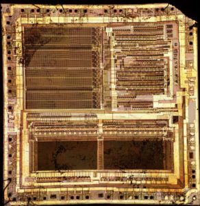
The PIC12CE518 microcontroller, widely used in embedded systems, stores critical firmware in its internal memory. Sometimes, due to corruption, loss of access, or the need for system modifications, there may be a need to recover or restore the chip’s binary. At [Your Company Name], we specialize in recovering the PIC12CE518 binary using advanced techniques to decode, decrypt, and reverse engineer the firmware, providing you with full access to your system’s data.
![Der Mikrocontroller PIC12CE518, der in eingebetteten Systemen weit verbreitet ist, speichert kritische Firmware in seinem internen Speicher. Manchmal kann es aufgrund von Beschädigungen, Zugriffsverlusten oder der Notwendigkeit von Systemänderungen erforderlich sein, die Binärdatei des Chips wiederherzustellen oder wiederherzustellen. Bei [Name Ihres Unternehmens] sind wir auf die Wiederherstellung der Binärdatei des PIC12CE518 spezialisiert und verwenden fortschrittliche Techniken zum Dekodieren, Entschlüsseln und Reverse Engineering der Firmware, sodass Sie vollen Zugriff auf die Daten Ihres Systems erhalten.](https://www.ic-crack.com/wp-content/uploads/2015/04/dscf4968_cropped-296x300.jpg)
Der Mikrocontroller PIC12CE518, der in eingebetteten Systemen weit verbreitet ist, speichert kritische Firmware in seinem internen Speicher. Manchmal kann es aufgrund von Beschädigungen, Zugriffsverlusten oder der Notwendigkeit von Systemänderungen erforderlich sein, die Binärdatei des Chips wiederherzustellen oder wiederherzustellen. Bei [Name Ihres Unternehmens] sind wir auf die Wiederherstellung der Binärdatei des PIC12CE518 spezialisiert und verwenden fortschrittliche Techniken zum Dekodieren, Entschlüsseln und Reverse Engineering der Firmware, sodass Sie vollen Zugriff auf die Daten Ihres Systems erhalten.
Our team of experts uses a series of sophisticated tools and methods to crack the chip’s security and break any obfuscation techniques protecting the firmware. We can reverse engineer the binary code from the PIC12CE518, even if the data has been intentionally encrypted or encoded. This process enables us to uncover valuable insights into how the system functions, detect potential vulnerabilities, and assist with debugging or customizing the firmware for your specific needs.
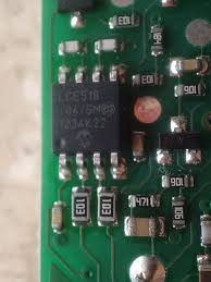
Нашият екип от експерти използва серия от усъвършенствани инструменти и методи, за да пробие сигурността на чипа и да разбие всички техники за обфускация, защитаващи фърмуера. Можем да проектираме обратно двоичния код от PIC12CE518, дори ако данните са умишлено криптирани или кодирани. Този процес ни позволява да разкрием ценна информация за това как функционира системата, да открием потенциални уязвимости и да помогнем при отстраняване на грешки или персонализиране на фърмуера за вашите специфични нужди.
Whether you need to attack a particular piece of firmware to extract sensitive information, hack into a locked system, or restore lost data, our services are tailored to handle complex challenges. We employ state-of-the-art methods to decrypt any protection schemes, ensuring a secure, efficient recovery process.
With our knowledge in embedded systems and microcontroller architectures, we can assist with various tasks, from decoding encrypted firmware to extracting the binary for modifications or audits. We understand the importance of confidentiality, security, and precision in these delicate processes.
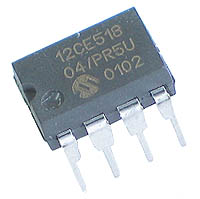
Cho dù bạn cần tấn công một phần chương trình cơ sở cụ thể để trích xuất thông tin nhạy cảm, hack vào hệ thống bị khóa hoặc khôi phục dữ liệu đã mất, các dịch vụ của chúng tôi đều được thiết kế riêng để xử lý các thách thức phức tạp. Chúng tôi sử dụng các phương pháp tiên tiến nhất để giải mã mọi chương trình bảo vệ, đảm bảo quy trình khôi phục an toàn và hiệu quả.
Với kiến thức về hệ thống nhúng và kiến trúc vi điều khiển, chúng tôi có thể hỗ trợ nhiều nhiệm vụ khác nhau, từ giải mã chương trình cơ sở được mã hóa đến trích xuất nhị phân để sửa đổi hoặc kiểm tra. Chúng tôi hiểu tầm quan trọng của tính bảo mật, an ninh và độ chính xác trong các quy trình tinh vi này.
As a program instruction is executed, the Program Counter (PC) will contain the address of the next program instruction to be executed by Recover Chip PIC12CE518 Binary. The PC value is increased by one every instruction cycle, unless an instruction changes the PC. For a GOTO instruction, bits 8:0 of the PC are provided by the GOTO instruction word. The PC Latch (PCL) is mapped to PC<7:0>. Bit 5 of the STATUS register provides page information to bit 9 of the PC (Figure 4- 8).
For a CALL instruction, or any instruction where the PCL is the destination, bits 7:0 of the PC again are provided by the instruction word. However, PC<8> does not come from the instruction word, but is always cleared.
Instructions where the PCL is the destination, or Modify PCL instructions, include MOVWF PC, ADDWF PC, and BSF PC,5.
The Program Counter is set upon a RESET, which means that the PC addresses the last location in the last page i.e., the oscillator calibration instruction. After executing MOVLW XX, the PC will roll over to location 00h, and begin executing user code.
The STATUS register page preselect bits are cleared upon a RESET, which means that page 0 is pre-selected.
Therefore, upon a RESET, a GOTO instruction will automatically cause the program to jump to page 0 until the value of the page bits is altered. PIC12C5XX devices have a 12-bit wide L.I.F.O. hardware push/pop stack to Attack IC PIC16C74B Binary.
A CALL instruction will push the current value of stack 1 into stack 2 and then push the current program counter value, incremented by one, into stack level 1. If more than two sequential CALL’s are executed, only the most recent two return addresses are stored when Recover Chip PIC12CE518 Binary.
ARETLW instruction will pop the contents of stack level 1 into the program counter and then copy stack level contents into level 1. If more than two sequential RETLW’s are executed, the stack will be filled with the address previously stored in level 2. Note that the W register will be loaded with the literal value specified in the instruction. This is particularly useful for the implementation of data look-up tables within the program memory when MCU Cracking.
Upon any reset, the contents of the stack remain unchanged, however the program counter (PCL) will also be reset.
 Recover Chip PIC16C554A Eeprom
The PIC16C55X(A) are 18 and 20-Pin EPROM-based members of the versatile PIC16CXX family of low-cost, high-performance, CMOS, fully-static, 8-bit microcontrollers. All PICmicro™ microcontrollers employ an advanced RISC architecture. The PIC16C55X(A) have enhanced core features, eight-level deep stack, and multiple internal and external interrupt sources which is critical for Recover Chip PIC16C554A Eeprom. The separate instruction and data buses of the Harvard architecture allow a 14-bit wide instruction word with the separate 8-bit wide data.
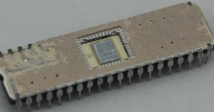
1. चिप पहचान और विश्लेषण
हम माइक्रोकंट्रोलर संस्करण की पहचान करके, मेमोरी संरचना का विश्लेषण करके और सक्रिय सुरक्षा लॉक की जाँच करके शुरू करते हैं। यह चरण संरक्षित डेटा को डिक्रिप्ट और निकालने के लिए सबसे अच्छी विधि निर्धारित करने में मदद करता है।
2. सुरक्षित EEPROM डेटा पढ़ना
विशेष चिप प्रोग्रामर का उपयोग करके, हम मानक और उन्नत निष्कर्षण तकनीकों दोनों के माध्यम से EEPROM और फ्लैश मेमोरी को पढ़ने का प्रयास करते हैं। यदि डेटा लॉक या एन्क्रिप्टेड है, तो हम उन्नत हैकिंग और डिकोडिंग विधियों पर आगे बढ़ते हैं।
3. सुरक्षा सुरक्षा को दरकिनार करना
PIC16C554A के सुरक्षा फ़्यूज़ फ़र्मवेयर स्रोत कोड, बाइनरी फ़ाइलों या EEPROM अभिलेखागार तक सीधी पहुँच को रोकते हैं। हमारे विशेषज्ञ निम्न के संयोजन का उपयोग करते हैं:
मेमोरी को अनलॉक करने के लिए चिप को धोखा देने के लिए वोल्टेज गड़बड़ाना
आंतरिक सर्किटरी तक भौतिक रूप से पहुँचने के लिए डिकैपिंग तकनीकें
निष्पादन का अनुकरण करने और सुरक्षित डेटा को पुनः प्राप्त करने के लिए फ़र्मवेयर इम्यूलेशन
4. डेटा निष्कर्षण और क्लोनिंग
एक बार जब सुरक्षित फ़र्मवेयर और EEPROM फ़ाइलों तक पहुँच हो जाती है, तो हम बाइनरी और हेक्सिमल डेटा को पढ़ने योग्य प्रारूप में डिक्रिप्ट, कॉपी और डुप्लिकेट करते हैं। यह क्लाइंट को खोई हुई फ़ाइलों को पुनर्स्थापित करने, फ़र्मवेयर व्यवहार का विश्लेषण करने या एम्बेडेड प्रोग्राम को संशोधित करने की अनुमति देता है।
5. रीप्रोग्रामिंग और बहाली
सफल EEPROM रिकवरी के बाद, निकाले गए डेटा को किसी अन्य संगत PIC16C554A माइक्रोकंट्रोलर पर रीफ्लैश, रिस्टोर या क्लोन किया जा सकता है। यह सिस्टम रिपेयर, फ़र्मवेयर अपग्रेड और कस्टम एम्बेडेड सॉल्यूशन विकसित करने के लिए उपयोगी है।
The two-stage instruction pipeline allows all instructions to execute in a single-cycle, except for program branches (which require two cycles). A total of 35 instructions (reduced instruction set) are available. Additionally, a large register set gives some of the architectural innovations used to achieve a very high performance after Crack MCU.
PIC16C55X(A) microcontrollers typically achieve a 2:1 code compression and a 4:1 speed improvement over other 8-bit microcontrollers in their class. The PIC16C554(A) and PIC16C556A have 80 bytes of RAM. The PIC16C558(A) has 128 bytes of RAM. Each device has 13 I/O pins and an 8-bit timer/counter with an 8-bit programmable prescaler.
PIC16C55X(A) devices have special features to reduce external components, thus reducing cost, enhancing system reliability and reducing power consumption. There are four oscillator options, of which the single pin RC oscillator provides a low-cost solution, the LP oscillator minimizes power consumption, XT is a standard crystal, and the HS is for High Speed crystals in order to Break MCU PIC16F946 Program. The SLEEP (power-down) mode offers power saving.
![Der Mikrocontroller PIC16C554A wird aufgrund seiner Zuverlässigkeit, seines geringen Stromverbrauchs und seiner vielseitigen Flash-Speicherarchitektur häufig in eingebetteten Systemen eingesetzt. Ist sein EEPROM-Speicher jedoch gesperrt, verschlüsselt oder geschützt, wird der Zugriff auf die gespeicherte Firmware, Binärdateien oder Programmdaten zu einer Herausforderung. [Ihr Firmenname] ist auf Reverse Engineering, Cracking und Entschlüsselung gesicherter Mikrocontroller spezialisiert und bietet Ihnen Expertendienste zur Wiederherstellung und Duplizierung der im PIC16C554A EEPROM gespeicherten Daten.](https://www.ic-crack.com/wp-content/uploads/2015/03/微信图片_20250217164113-300x112.png)
Der Mikrocontroller PIC16C554A wird aufgrund seiner Zuverlässigkeit, seines geringen Stromverbrauchs und seiner vielseitigen Flash-Speicherarchitektur häufig in eingebetteten Systemen eingesetzt. Ist sein EEPROM-Speicher jedoch gesperrt, verschlüsselt oder geschützt, wird der Zugriff auf die gespeicherte Firmware, Binärdateien oder Programmdaten zu einer Herausforderung. [Ihr Firmenname] ist auf Reverse Engineering, Cracking und Entschlüsselung gesicherter Mikrocontroller spezialisiert und bietet Ihnen Expertendienste zur Wiederherstellung und Duplizierung der im PIC16C554A EEPROM gespeicherten Daten.
A UV-erasable CERDIP-packaged version is ideal for code development while the cost-effective One-Time Programmable (OTP) version is suitable for production in any volume to faciliate the process of Break IC PIC16F917 Heximal.
![PIC16C554A माइक्रोकंट्रोलर अपनी विश्वसनीयता, कम बिजली की खपत और बहुमुखी फ्लैश मेमोरी आर्किटेक्चर के कारण एम्बेडेड सिस्टम में व्यापक रूप से उपयोग किया जाता है। हालाँकि, जब इसकी EEPROM मेमोरी लॉक, एन्क्रिप्टेड या संरक्षित होती है, तो संग्रहीत फ़र्मवेयर, बाइनरी फ़ाइलें या प्रोग्राम डेटा तक पहुँचना एक चुनौती बन जाती है। [आपकी कंपनी का नाम] में, हम रिवर्स इंजीनियरिंग, क्रैकिंग और सुरक्षित माइक्रोकंट्रोलर को डिक्रिप्ट करने में विशेषज्ञ हैं, जो PIC16C554A EEPROM में संग्रहीत डेटा को पुनर्प्राप्त करने, पुनर्स्थापित करने और डुप्लिकेट करने के लिए विशेषज्ञ सेवाएँ प्रदान करते हैं।](https://www.ic-crack.com/wp-content/uploads/2015/03/v2-af3d082248d7e9e2174ebe8ee0dbe000_r-1-300x225.jpg)
PIC16C554A माइक्रोकंट्रोलर अपनी विश्वसनीयता, कम बिजली की खपत और बहुमुखी फ्लैश मेमोरी आर्किटेक्चर के कारण एम्बेडेड सिस्टम में व्यापक रूप से उपयोग किया जाता है। हालाँकि, जब इसकी EEPROM मेमोरी लॉक, एन्क्रिप्टेड या संरक्षित होती है, तो संग्रहीत फ़र्मवेयर, बाइनरी फ़ाइलें या प्रोग्राम डेटा तक पहुँचना एक चुनौती बन जाती है। [आपकी कंपनी का नाम] में, हम रिवर्स इंजीनियरिंग, क्रैकिंग और सुरक्षित माइक्रोकंट्रोलर को डिक्रिप्ट करने में विशेषज्ञ हैं, जो PIC16C554A EEPROM में संग्रहीत डेटा को पुनर्प्राप्त करने, पुनर्स्थापित करने और डुप्लिकेट करने के लिए विशेषज्ञ सेवाएँ प्रदान करते हैं।
 Recover MCU PIC16CR84 Code
We can Recover MCU PIC16CR84 Code, please view the MCU PIC16CR84 features for your reference:
A variety of frequency ranges and packaging options are available. Depending on application and production requirements the proper device option can be selected using the information in this section.
When placing orders, please use the “PIC16F8X Product Identification System” at the back of this data sheet to specify the correct part number.
There are four device “types” as indicated in the device number.
1. F, as in PIC16F84. These devices have Flash program memory and operate over the standard voltage range after Attack MCU firmware.
2. LF, as in PIC16LF84. These devices have Flash program memory and operate over an extended voltage range.
3. CR, as in PIC16CR83. These devices have ROM program memory and operate over the standard voltage range.
4. LCR, as in PIC16LCR84. These devices have ROM program memory and operate over an extended voltage range.
When discussing memory maps and other architectural features, the use of F and CR also implies the LF and LCR versions.
2.1 Flash Devices
These devices are offered in the lower cost plastic package, even though the device can be erased and reprogrammed. This allows the same device to be used for prototype development and pilot programs as well as production after Recover MCU.
A further advantage of the electrically-erasable Flash version is that it can be erased and reprogrammed in-circuit, or by device programmers, such as Microchip’s PICSTART® Plus or PRO MATE® II programmers.
2.2 Quick-Turnaround-Production (QTP) Devices
Microchip offers a QTP Programming Service for factory production orders. This service is made available for users who choose not to program a medium to high quantity of units and whose code patterns have stabilized.
The devices have all Flash locations and configuration options already programmed by the factory. Certain code and prototype verification procedures do apply before production shipments are available.
2.3 Serialized Quick-Turnaround-Production (SQTP SM ) Devices
Microchip offers the unique programming service where a few user-defined locations in each device are programmed with different serial numbers. The serial numbers may be random, pseudo-random or sequential if Copy MCU Firmware.
Serial programming allows each device to have a unique number which can serve as an entry-code, password or ID number.
Some of Microchip’s devices have a corresponding device where the program memory is a ROM. These devices give a cost savings over Microchip’s traditional user programmed devices (EPROM, EEPROM).
ROM devices (PIC16CR8X) do not allow serialization information in the program memory space. The user may program this information into the Data EEPROM when Recover MCU PIC16CR84 Code.
The high performance of the PIC16CXX family can be attributed to a number of architectural features commonly found in RISC microprocessors. To begin with, the PIC16CXX uses a Harvard architecture.
This architecture has the program and data accessed from separate memories. So the device has a program memory bus and a data memory bus. This improves bandwidth over traditional von Neumann architecture where program and data are fetched from the same memory (accesses over the same bus).
Separating program and data memory further allows instructions to be sized differently than the 8-bit wide data word. PIC16CXX opcodes are 14-bits wide, enabling single word instructions to Crack MCU.
The full 14-bit wide program memory bus fetches a 14-bit instruction in a single cycle. A two-stage pipeline overlaps fetch and execution of instructions (see below picture).
Consequently, all instructions execute in a single cycle except for program branches.
The PIC16F83 and PIC16CR83 address 512 x 14 of program memory, and the PIC16F84 and PIC16CR84 address 1K x 14 program memory. All program memory is internal.
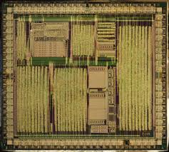
 Reverse Engineering Microcontroller PIC16CR83 Heximal
We can Reverse Engineering Microcontroller PIC16CR83 Heximal, please view the Microcontroller PIC16CR83 features for your refernece:
A variety of frequency ranges and packaging options are available. Depending on application and production requirements the proper device option can be selected using the information in this section. When placing orders, please use the “PIC16F8X Product Identification System” at the back of this data sheet to specify the correct part number.
There are four device “types” as indicated in the device number.
1. F, as in PIC16F84. These devices have Flash program memory and operate over the standard voltage range.
2. LF, as in PIC16LF84. These devices have Flash;
3. CR, as in PIC16CR83. These devices have ROM program memory and operate over the standard voltage range.
LCR, as in PIC16LCR84. These devices have ROM program memory and operate over an extended voltage range.
When discussing memory maps and other architectural features, the use of F and CR also implies the LF and LCR versions.
These devices are offered in the lower cost plastic package, even though the device can be erased and reprogrammed to ease the process of EPROM advantage when MCU Code Decryption. This allows the same device to be used for prototype development and pilot programs as well as production.
Reverse Engineering Microcontroller PIC16CR83 Heximal
A further advantage of the electrically-erasable Flash version is that it can be erased and reprogrammed in-circuit, or by device programmers, such as Microchip’s PICSTART® Plus or PRO MATE® II programmers.
2.2 Quick-Turnaround-Production (QTP) Devices
Microchip offers a QTP Programming Service for factory production orders. This service is made available for users who choose not to program a medium to high quantity of units and whose code patterns have stabilized. The devices have all Flash locations and configuration options already programmed by the factory. Certain code and prototype verification procedures do apply to IC Code Break’s intermediate approach before production shipments are available.
Microchip offers the unique programming service where a few user-defined locations in each device are programmed with different serial numbers. The serial numbers may be random, pseudo-random or sequential.
Serial programming allows each device to have a unique number which can serve as an entry-code, password or ID number when Crack MCU. Device where the program memory is a ROM. These Some of Microchip’s devices have a corresponding devices give a cost savings over Microchip’s traditional user programmed devices (EPROM, EEPROM). ROM devices (PIC16CR8X) do not allow serialization information in the program memory space. The user may program this information into the Data EEPROM.
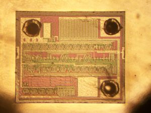
 Recover MCU PIC16C712 Binary
We can Recover MCU PIC16C712 Binary, please view the MCU PIC16C712 features for your reference:
Microcontroller Core Features:
· High-performance RISC CPU
· Only 35 single word instructions to learn
· All single cycle instructions except for program branches which are two cycle
· Operating speed: DC – 20 MHz clock input DC – 200 ns instruction cycle
· Interrupt capability (up to 7 internal/external interrupt sources) which can be applied for Microcontroller Unlocking
· Eight level deep hardware stack
· Direct, indirect and relative addressing modes
· Power-on Reset (POR)
· Power-up Timer (PWRT) and Oscillator Start-up Timer (OST)
· Watchdog Timer (WDT) with its own on-chip RC oscillator for reliable operation
· Brown-out detection circuitry for Brown-out Reset (BOR)
· Programmable code-protection against Break Microcontroller PIC16F886 Software
· Power saving SLEEP mode
· Selectable oscillator options
· Low-power, high-speed CMOS EPROM technology
· Fully static design
· In-Circuit Serial Programming (ICSP)
· Wide operating voltage range: 2.5V to 5.5V
· High Sink/Source Current 25/25 mA
· Commercial, Industrial and Extended temperature ranges
· Low-power consumption:
– < 2 mA @ 5V, 4 MHz
– 22.5 µA typical @ 3V, 32 kHz
– < 1 µA typical standby current
Peripheral Features:
· Timer0: 8-bit timer/counter with 8-bit prescaler
· Timer1: 16-bit timer/counter with prescaler can be incremented during sleep via external crystal/clock
· Timer2: 8-bit timer/counter with 8-bit period register, prescaler and postscaler after Recover IC PIC16C73B Firmware
· Capture, Compare, PWM module
· Capture is 16-bit, max. resolution is 12.5 ns, Compare is 16-bit, max. resolution is 200 ns, PWM maximum resolution is 10-bit
· 8-bit multi-channel Analog-to-Digital converter
Recover MCU PIC16C712 Binary
This document contains device-specific information. Additional information may be found in the PICmicro™ Mid-Range Reference Manual, (DS33023), which may be obtained from your local Microchip Sales Representative or downloaded from the Microchip website. The Reference Manual should be considered a complementary document to this datasheet, and is highly recommended reading for a better understanding of the device architecture and operation of the peripheral modules.
 Recover Chip PIC16C71 Code
We can Recover Chip PIC16C71 Code, please view the Chip PIC16C71 features for your reference:
The PIC16C71X is a family of low-cost, high-performance, CMOS, fully-static, 8-bit microcontrollers with integrated analog-to-digital (A/D) converters, in the PIC16CXX mid-range family.
All PIC16/17 microcontrollers employ an advanced RISC architecture. The PIC16CXX microcontroller family has enhanced core features, eight-level deep stack, and multiple internal and external interrupt sources which can be applied for Microcontroller Unlocking.
The separate instruction and data buses of the Harvard architecture allow a 14-bit wide instruction word with the separate 8-bit wide data. The two stage instruction pipeline allows all instructions to execute in a single cycle, except for program branches which require two cycles after Recover Chip PIC16C71 Code.
A total of 35 instructions (reduced instruction set) are available. Additionally, a large register set gives some of the architectural innovations used to achieve a very high performance. PIC16CXX microcontrollers typically achieve a 2:1 code compression and a 4:1 speed improvement over other 8-bit microcontrollers in their class, The PIC16C710/71 devices have 36 bytes of RAM, the PIC16C711 has 68 bytes of RAM and the PIC16C715 has 128 bytes of RAM.
Each device has 13 I/O pins. In addition a timer/counter is available. Also a 4-channel high-speed 8-bit A/D is provided which can be used for Recover IC PIC16F72A Binary. The 8-bit resolution is ideally suited for applications requiring low-cost analog interface, e.g. thermostat control, pressure sensing, etc.
The PIC16C71X family has special features to reduce external components, thus reducing cost, enhancing system reliability and reducing power consumption.
There are four oscillator options, of which the single pin RC oscillator provides a low-cost solution, the LP oscillator minimizes power consumption in order to Break Microcontroller PIC16C65B Eeprom, XT is a standard crystal, and the HS is for High Speed crystals only.
The SLEEP (power-down) feature provides a power saving mode. The user can wake up the chip from SLEEP through several external and internal interrupts and resets.
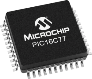
 Recover Chip PIC16C77 Flash
There are actually two 8-bit latches, one for data-out (from the PIC16/17) and one for data input. The user writes 8-bit data to PORTD data latch and Recover Chip PIC16C77 Flash. Chip Select from the port pin latch (note that they have the same address). In this mode, the TRISD register is ignored, since the microprocessor is controlling the direction of A write to the PSP occurs when both the CS and WR lines are first detected low. When either the CS or WR lines become high (level triggered), then the Input Buffer Full status flag bit IBF (TRISE<7>) is set on the Q4 clock cycle, following the next Q2 cycle, to signal the write is complete.
Recover Chip PIC16C77 Flash
The interrupt flag bit PSPIF (PIR1<7>) is also set on the same Q4 clock cycle. IBF can only be cleared by reading the PORTD input latch. The input Buffer Overflow status flag bit IBOV (TRISE<5>) is set if a second write to the Parallel Slave Port is attempted when the previous byte has not been read out of the buffer.
A read from the PSP occurs when both the CS and RD lines are first detected low. The Output Buffer Full status flag bit OBF (TRISE<6>) is cleared immediately indicating that the PORTD latch is waiting to be read by the external bus.
When either the CS or RD pin becomes high (level triggered), the interrupt flag bit PSPIF is set on the Q4 clock cycle, following the next Q2 cycle, indicating that the read is complete. OBF remains low until data is written to PORTD by the user firmware.
When not in Parallel Slave Port mode, the IBF and OBF bits are held clear. However, if flag bit IBOV was previously set, it must be cleared in firmware. An interrupt is generated and latched into flag bit PSPIF when a read or write operation is completed. PSPIF must be cleared by the user in firmware and the interrupt can be disabled by clearing the interrupt enable bit PSPIE (PIE1<7>).
The Timer0 module is a simple 8-bit overflow counter.
The clock source can be either the internal system clock (Fosc/4) or an external clock. When the clock CCP Overview source is an external clock, the Timer0 module can be selected to increment on either the rising or falling edge.
The Timer0 module also has a programmable prescaler option. This prescaler can be assigned to either the Timer0 module or the Watchdog Timer. Bit PSA (OPTION<3>) assigns the prescaler, and bits PS2:PS0 (OPTION<2:0>) determine the prescaler value.
Timer0 can increment at the following rates: 1:1 (when pres-caler assigned to Watchdog timer), 1:2, 1:4, 1:8, 1:16, 1:32, 1:64, 1:128, and 1:256 (Timer0 only). Synchronization of the external clock occurs after the prescaler. When the prescaler is used, the external clock frequency may be higher then the device’s frequency.
The maximum frequency is 50 MHz, given the high and low time requirements of the clock Timer1 is a 16-bit timer/counter. The clock source can be either the internal system clock (Fosc/4), an external clock, or an external crystal.
Timer1 can operate as either a timer or a counter. When operating as a counter (external clock source) when Recover Chip, the counter can either operate synchronized to the device or asynchronously to the device.
Asynchronous operation allows Timer1 to operate during sleep, which is useful for applications that require a real-time clock as well as the power savings of SLEEP mode. Timer1 also has a prescaler option which allows Timer1 to increment at the following rates: 1:1, 1:2, 1:4, and 1:8. Timer1 can be used in conjunction with the Capture/Compare/PWM module.
When used with a CCP module, Timer1 is the time-base for 16-bit Capture or the 16-bit Compare and must be synchronized to the device by Recover Chip PIC16C77 Flash. The CCP module(s) can operate in one of these three modes: 16-bit capture, 16-bit compare, or up to 10-bit Pulse Width Modulation (PWM).
Capture mode captures the 16-bit value of TMR1 into the CCPRxH:CCPRxL register pair. The capture event can be programmed for either the falling edge, rising edge, fourth rising edge, or the sixteenth rising edge of the CCPx pin. Compare mode compares the TMR1H:TMR1L register pair to the CCPRxH:CCPRxL register pair. When a match occurs an interrupt can be generated by Crack MCU, and the output pin CCPx can be forced to given state (High or Low), TMR1 can be reset (CCP1), or TMR1 reset and start A/D conversion (CCP2).
This depends on the control bits CCPxM3:CCPxM0. PWM mode compares the TMR2 register to a 10-bit duty cycle register (CCPRxH:CCPRxL<5:4>).
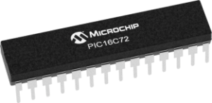
 Recover MCU PIC16C72 Software
We can Recover MCU PIC16C72 Software, please see the MCU PIC16C72 features for your reference:
PIC16C7X Microcontroller Core Features:
· High-performance RISC CPU
· Only 35 single word instructions to learn
· All single cycle instructions except for program branches which are two cycle
· Operating speed: DC – 20 MHz clock input DC – 200 ns instruction cycle
· Up to 8K x 14 words of Program Memory, up to 368 x 8 bytes of Data Memory (RAM)
· Interrupt capability
· Eight level deep hardware stack
· Direct, indirect, and relative addressing modes
· Power-on Reset (POR) to facilitate the process of Recover Chip PIC16C73B Firmware
· Power-up Timer (PWRT) and Oscillator Start-up Timer (OST)
· Watchdog Timer (WDT) with its own on-chip RC oscillator for reliable operation
· Programmable code-protection
· Power saving SLEEP mode
· Selectable oscillator options
· Low-power, high-speed CMOS EPROM technology which is quite common for MCU Cracking
· Fully static design
· Wide operating voltage range: 2.5V to 6.0V
· High Sink/Source Current 25/25 mA
· Commercial, Industrial and Extended temperature ranges
· Low-power consumption:
· < 2 mA @ 5V, 4 MHz
· 15 µA typical @ 3V, 32 kHz
· < 1 µA typical standby current
PIC16C7X Peripheral Features:
· Timer0: 8-bit timer/counter with 8-bit prescaler
· Timer1: 16-bit timer/counter with prescaler, can be incremented during sleep via external crystal/clock
· Timer2: 8-bit timer/counter with 8-bit period register, prescaler and postscaler
· Capture, Compare, PWM module(s)
Recover MCU PIC16C72 Software
· Capture is 16-bit, max. resolution is 12.5 ns, Compare is 16-bit, max. resolution is 200 ns, PWM max. resolution is 10-bit
· 8-bit multichannel analog-to-digital converter
· Synchronous Serial Port (SSP) with SPI and I2C
· Universal Synchronous Asynchronous Receiver Transmitter (USART/SCI)
· Parallel Slave Port (PSP) 8-bits wide, with external RD, WR and CS controls before Recover MCU PIC16C63A Firmware
· Brown-out detection circuitry for Brown-out Reset (BOR)
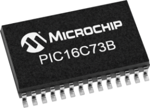
 Recover Chip PIC16C73B Firmware
A highly reliable Watchdog Timer (WDT), with its own on-chip RC oscillator, provides protection against software lockup when Recover Chip PIC16C73B Firmware, and also provides one way of waking the device from SLEEP. A UV erasable CERDIP packaged version is ideal for code development, while the cost effective One-Time-Programmable (OTP) version is suitable for production in any volume.
The PIC16C73B devices fit nicely in many applications ranging from security and remote sensors to appliance control and automotive. The EPROM technology makes customization of application programs (transmitter codes, motor speeds, receiver frequencies, etc.) extremely fast and convenient.
The small footprint packages make this microcontroller series perfect for all applications with space limitations. Low cost, low power, high performance, ease of use and I/O flexibility make the PIC16C65B devices very versatile, even in areas where no microcontroller use has been considered before (e.g., timer functions, serial communication, capture and compare, PWM functions and coprocessor applications).
Users familiar with the PIC16C5X microcontroller family will realize that this is an enhanced version of the PIC16C5X architecture. Please refer to Appendix A for a detailed list of enhancements. Code written for the PIC16C5X can be easily ported to the PIC16CXX family of devices which can be used for Recover MCU 12F508 Code.
Recover Chip PIC16C73B Firmware
PICmicro® devices are supported by the complete line of Microchip Development tools. Please refer to Section 15.0 for more details about Microchip’s development tools which can also being used for Microcontroller Unlocking.
A variety of frequency ranges and packaging options are available. Depending on application and production requirements, the proper device option can be selected using the information in the PIC16C73B Product Identification System section at the end of this data sheet.
When placing orders, please use that page of the data sheet to specify the correct part number. For the PIC16C7X family, there are two device “types” as indicated in the device number.
