Archive for the ‘Recover Chip’ Category
 Recovery Microcontroller ATmega48A Program
The Bit Copy instructions BLD (Bit LoaD) and BST (Bit STore) use the T-bit as source or destination for the operated bit. A bit from a register in the Register File can be copied into T by the BST instruction after , and a bit in T can be copied into a bit in a register in the Register File by the BLD instruction.
Bit 5 – H: Half Carry Flag
The Half Carry Flag H indicates a Half Carry in some arithmetic operations. Half Carry Is useful in BCD arithmetic. See the “Instruction Set Description” for detailed information.
Bit 4 – S: Sign Bit, S = N ⊕ V
The S-bit is always an exclusive or between the Negative Flag N and the Two’s Complement Overflow Flag V. See the “Instruction Set Description” for detailed information.
Bit 3 – V: Two’s Complement Overflow Flag
The Two’s Complement Overflow Flag V supports two’s complement arithmetics. See the “Instruction Set Description” for detailed information.
Bit 2 – N: Negative Flag
The Negative Flag N indicates a negative result in an arithmetic or logic operation. See the “Instruction Set Description” for detailed information.
Bit 1 – Z: Zero Flag
The Zero Flag Z indicates a zero result in an arithmetic or logic operation. See the “Instruction Set Description” for detailed information.
Bit 0 – C: Carry Flag
The Carry Flag C indicates a carry in an arithmetic or logic operation. See the “Instruction Set Description” for detailed information.
The Register File is optimized for the AVR Enhanced RISC instruction set in the purpose of Break PIC18F4331 Microprocessor Eeprom Memory. In order to achieve the required performance and flexibility, the following input/output schemes are supported by the Register File:
One 8-bit output operand and one 8-bit result input
Two 8-bit output operands and one 8-bit result input
Two 8-bit output operands and one 16-bit result input
One 16-bit output operand and one 16-bit result input
Figure 5-2 shows the structure of the 32 general purpose working registers in the CPU.
Програма відновлення мікроконтролера ATmega48A передбачає розширені методи злому та декодування зашифрованого та заблокованого мікропрограмного забезпечення, що зберігається в його захищеній флеш-пам’яті та пам’яті EEPROM. Будучи захисним мікроконтролером (MCU), ATmega48A містить надійні функції безпеки для захисту своїх двійкових і шістнадцяткових даних, що робить зворотне проектування необхідним для законних цілей, таких як відновлення функціональності або клонування вбудованого програмного забезпечення.
Most of the instructions operating on the Register File have direct access to all registers, and most of them are single cycle instructions.
Each register is also assigned a data memory address, mapping them directly into the first 32 locations of the user Data Space. Although not being physically implemented as SRAM locations only when Microprocessor PIC18F2515 Heximal File Recovery, this memory organization provides great flexibility in access of the registers, as the X-, Y- and Z-pointer registers can be set to index any register in the file.
The registers R26..R31 have some added functions to their general purpose usage. These registers are 16-bit address pointers for indirect addressing of the data space. The three indirect address registers X, Y, and Z are defined as described in Figure 5-3.
The Stack is mainly used for storing temporary data, for storing local variables and for storing return addresses after interrupts and subroutine calls. The Stack Pointer Register always points to the top of the Stack. Note that the Stack is implemented as growing from higher memory locations to lower memory locations. This implies that a Stack PUSH command decreases the Stack Pointer.
The Stack Pointer points to the data SRAM Stack area where the Subroutine and Interrupt Stacks are located. This Stack space in the data SRAM must be defined by the program before any subroutine calls are executed or interrupts are enabled to provide greater support for Break Microcontroller TI TMS320F28232PGFA Protection. The Stack Pointer must be set to point above 0x0100, preferably RAMEND.
The Stack Pointer is decremented by one when data is pushed onto the Stack with the PUSH instruction, and it is decremented by two when the return address is pushed onto the Stack with subroutine call or interrupt. The Stack Pointer is incremented by one when data is popped from the Stack with the POP instruction, and it is incremented by two when data is popped from the Stack with return from subroutine RET or return from interrupt RETI.
بازیابی میکروکنترلر برنامه ATmega48A شامل روش های پیشرفته ای برای کرک و رمزگشایی سیستم عامل رمزگذاری شده و قفل شده ذخیره شده در حافظه فلش ایمن و حافظه EEPROM است. به عنوان یک میکروکنترلر محافظ (MCU)، ATmega48A دارای ویژگیهای امنیتی قوی برای محافظت از دادههای باینری و هگزیمال خود است، که مهندسی معکوس را برای اهداف قانونی مانند بازیابی عملکرد یا شبیهسازی نرمافزار تعبیهشده ضروری میسازد.
The AVR Stack Pointer is implemented as two 8-bit registers in the I/O space. The number of bits actually used is implementation dependent. Note that the data space in some implementations of the AVR architecture is so small that only SPL is needed when Crack MCU firmware. In this case, the SPH Register will not be present.
 Recover Microcontroller ATmega64pa Binary
The ATmega64 is a highly complex microcontroller where the number of I/O locations supersedes the 64 I/O location reserved in the AVR instruction set which provide great convenience of Recover Microcontroller Atmega64pa Binary. To ensure backward compatibility with the ATmega103, all I/O locations present in ATmega103 have the same location in ATmega64.
Most additional I/O locations are added in an Extended I/O space starting from 0x60 to 0xFF (i.e., in the ATmega103 internal RAM space). These location can be reached by using LD/LDS/LDD and ST/STS/STD instructions only, not by using IN and OUT instructions to facilitate the progress of Break MCU MC68HC11F1CFN3 Heximal. The relocation of the internal RAM space may still be a problem for ATmega103 users.
Also, the increased number of Interrupt Vectors might be a problem if the code uses absolute addresses. To solve these problems, an ATMEGA64PA compatibility mode can be selected by programming the fuse M103C. In this mode, none of the functions in the Extended I/O space are in use, so the internal RAM is located as in ATMEGA64PA.
Also, the extended Interrupt Vectors are removed for the purpose of Break Chip PIC12C509 Code. The ATMEGA64PA is 100% pin compatible with ATMEGA64PA, and can replace the ATmega103 on current printed circuit boards. The application notes “Replacing ATmega103 by ATmega128” and “Migration between ATmega64 and ATmega128” describes what the user should be aware of replacing the ATmega103 by an ATmega128 or ATmega64.
By programming the M103C Fuse, the ATmega64 will be compatible with the ATmega103 regards to RAM, I/O pins and Interrupt Vectors as described above. However, some new features in ATmega64 are not available in this compatibility mode, these features are listed:
Pin Descriptions
One USART instead of two, asynchronous mode only. Only the eight least significant bits of the Baud Rate Register is available. One 16 bits Timer/Counter with two compare registers instead of two 16 bits Timer/Counters with three compare registers. Two-wire serial interface is not supported by Crack MCU Memory.
Port G serves alternate functions only (not a general I/O port). Port F serves as digital input only in addition to analog input to the ADC. Boot Loader capabilities is not supported. It is not possible to adjust the frequency of the internal calibrated RC Oscillator in order to Recover Microcontroller Atmega64pa Binary. The External Memory Interface can not release any Address pins for general I/O, neither configure different wait states to different External Memory Address sections.
Only EXTRF and PORF exist in the MICROCONTROLLER CSR Register. No timed sequence is required for Watchdog Timeout change. Only low-level external interrupts can be used on four of the eight External Interrupt sources. Port C is output only. USART has no FIFO buffer, so Data OverRun comes earlier. The user must have set unused I/O bits to 0 in ATmega103 programs.
 Recover Microcontroller ATmega32PA Firmware
We can Recover Microcontroller ATmega32PA Firmware, please view the Microcontroller ATmega32PA features for your reference:
Port A serves as the analog inputs to the A/D Converter.
Port A also serves as an 8-bit bi-directional I/O port, if the A/D Converter is not used. Port pins can provide internal pull-up resistors (selected for each bit). The Port A output buffers have symmetrical drive characteristics with both high sink and source capability.
When pins PA0 to PA7 are used as inputs and are externally pulled low, they will source current if the internal pull-up resistors are activated. The Port A pins are tri-stated when a reset condition becomes active, even if the clock is not running before Extract PLD IC Source Code.
Port B is an 8-bit bi-directional I/O port with internal pull-up resistors (selected for each bit). The Port B output buffers have symmetrical drive characteristics with both high sink and source capability. As inputs, Port B pins that are externally pulled low will source current if the pull-up resistors are activated.
The Port B pins are tri-stated when a reset condition becomes active, even if the clock is not running. Port C is an 8-bit bi-directional I/O port with internal pull-up resistors (selected for each bit). The Port C output buffers have symmetrical drive characteristics with both high sink and source capability. As inputs, Port C pins that are externally pulled low will source current if the pull-up resistors are activated before Break IC ATmega32A Software.
The Port C pins are tri-stated when a reset condition becomes active, even if the clock is not running. If the JTAG interface is enabled, the pull-up resistors on pins PC5(TDI), PC3(TMS) and PC2(TCK) will be activated even if a reset occurs. The TD0 pin is tri-stated unless TAP states that shift out data are entered.
Port D is an 8-bit bi-directional I/O port with internal pull-up resistors (selected for each bit). The Port D output buffers have symmetrical drive characteristics with both high sink and source capability. As inputs, Port D pins that are externally pulled low will source current if the pull-up resistors are activated.
The Port D pins are tri-stated when a reset condition becomes active, even if the clock is not running. Reset Input. A low level on this pin for longer than the minimum pulse length will generate a reset, even if the clock is not running. The minimum pulse length is given in Table 15 on page 37.
Shorter pulses are not guaranteed to generate a reset. Input to the inverting Oscillator amplifier and input to the internal clock operating circuit Output from the inverting Oscillator amplifier. AVCC is the supply voltage pin for Port A and the A/D Converter. It should be externally connected to VCC, even if the ADC is not used. If the ADC is used, it should be connected to VCC through a low-pass filter.
AREF is the analog reference pin for the A/D Converter. A comprehensive set of development tools, application notes and datasheets are available for download on http://www.atmel.com/avr. This documentation contains simple code examples that briefly show how to use various parts of the device. These code examples assume that the part specific header file is included before compilation after MCU Cracking Process. Be aware that not all C Compiler vendors include bit definitions in the header files and interrupt handling in C is compiler dependent.
 Recover Microcontroller ATmega16A Software
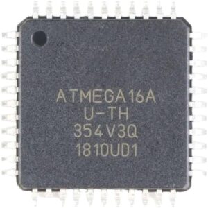
Recovering microcontroller ATmega16A software involves cracking or decoding the secured firmware stored in the secured MCU’s flash memory and EEPROM memory. The ATmega16A, like many MCUs, is designed with protective features to lock its binary and heximal data, making it challenging to access the embedded software without proper tools and techniques. To unlock the firmware, reverse engineering methods are often employed to bypass encryption protocols and retrieve the source code.
Il recupero del software del microcontrollore ATmega16A comporta il cracking o la decodifica del firmware protetto archiviato nella memoria flash e nella memoria EEPROM dell’MCU protetta. L’ATmega16A, come molti MCU, è progettato con funzionalità di protezione per bloccare i suoi dati binari ed esadecimali, rendendo difficile l’accesso al software incorporato senza strumenti e tecniche adeguati. Per sbloccare il firmware, vengono spesso impiegati metodi di reverse engineering per bypassare i protocolli di crittografia e recuperare il codice sorgente.
Once the locked software is unlocked, it can be restored to its original functionality, or cloned for use in other systems. This process is crucial when the program has been corrupted, lost, or when hardware replication is necessary. By extracting and recovering the program, engineers can ensure that systems relying on the ATmega16A MCU can continue operating without the need for expensive replacements.
However, recovering software from a microcontroller must be done ethically, ensuring compliance with legal standards regarding intellectual property rights.
We can Recover Microcontroller ATmega16A Software, please view the Microcontroller ATmega16A features for your reference:
First Analog Comparator conversion may be delayed
If the device is powered by a slow rising VCC, the first Analog Comparator conversion will take longer than expected on some devices.
Problem Fix/Workaround
When the device has been powered or reset, disable then enable theAnalog Comparator before the first conversion. Interrupts may be lost when writing the timer registers in the asynchronous time to Break IC PIC16C74 Code. The interrupt will be lost if a timer register that is synchronized to the asynchronous timer clock is written when the asynchronous Timer/Counter register(TCNTx) is 0x00 if Recover Microcontroller ATmega16A Software.
माइक्रोकंट्रोलर ATmega16A सॉफ़्टवेयर को पुनर्प्राप्त करने में सुरक्षित MCU की फ़्लैश मेमोरी और EEPROM मेमोरी में संग्रहीत सुरक्षित फ़र्मवेयर को क्रैक या डिकोड करना शामिल है। कई MCU की तरह, ATmega16A को इसके बाइनरी और हेक्सिमल डेटा को लॉक करने के लिए सुरक्षात्मक सुविधाओं के साथ डिज़ाइन किया गया है, जिससे उचित उपकरणों और तकनीकों के बिना एम्बेडेड सॉफ़्टवेयर तक पहुँचना चुनौतीपूर्ण हो जाता है। फ़र्मवेयर को अनलॉक करने के लिए, एन्क्रिप्शन प्रोटोकॉल को बायपास करने और स्रोत कोड को पुनः प्राप्त करने के लिए अक्सर रिवर्स इंजीनियरिंग विधियों का उपयोग किया जाता है।
Problem Fix / Workaround
Always check that the asynchronous Timer/Counter register neither have the value 0xFF nor 0x00 before writing to the asynchronous Timer Control Register(TCCRx), asynchronous Timer Counter Register(TCNTx), or asynchronous Output Compare Register(OCRx) for the purpose of Copy Chip PIC16C73A Program.
IDCODE masks data from TDI input
The JTAG instruction IDCODE is not working correctly. Data to succeeding devices are replaced by all-ones during Update-DR.
Problem Fix / Workaround
If ATmega16 is the only device in the scan chain, the problem is not visible.
Select the Device ID Register of the ATmega16 by issuing the IDCODE instruction or by entering the Test-Logic-Reset state of the TAP controller to recover out the contents of its Device ID Register and possibly data from succeeding devices of the scan chain. Issue the BYPASS instruction to the ATmega16 while recovering the Device ID Registers of preceding devices of the boundary scan chain before Recover Microcontroller ATmega16A Software.
If the Device IDs of all devices in the boundary scan chain must be captured simultaneously, the ATmega16 must be the fist device in the chain of Reverse Engineering Microcontroller PIC16F73 Program.
Recovering EEPROM by using ST or STS to set EERE bit triggers unexpected interrupt request.
Recovering EEPROM by using the ST or STS command to set the EERE bit in the EECR register triggers an unexpected EEPROM interrupt request.
Problem Fix / Workaround
Always use OUT or SBI to set EERE in EECR.
First Analog Comparator conversion may be delayed to Unlock Microcontroller, Interrupts may be lost when writing the timer registers in the asynchronous timer IDCODE masks data from TDI input
نرم افزار بازیابی میکروکنترلر ATmega16A شامل شکستن یا رمزگشایی سیستم عامل ایمن ذخیره شده در حافظه فلش MCU ایمن و حافظه EEPROM است. ATmega16A، مانند بسیاری از MCU ها، با ویژگی های محافظتی طراحی شده است تا داده های باینری و هگزیمال خود را قفل کند، و دسترسی به نرم افزار تعبیه شده بدون ابزار و تکنیک های مناسب را دشوار می کند. برای باز کردن قفل سفتافزار، اغلب از روشهای مهندسی معکوس برای دور زدن پروتکلهای رمزگذاری و بازیابی کد منبع استفاده میشود.
Recovering EEPROM by using ST or STS to set EERE bit triggers unexpected interrupt request. First Analog Comparator conversion may be delayed before Recover Microcontroller ATmega16A Software
If the device is powered by a slow rising VCC, the first Analog Comparator conversion will take longer than expected on some devices after Recover MCU PIC16C72 Software.
Problem Fix/Workaround
When the device has been powered or reset, disable then enable theAnalog Comparator before the first conversion.
 Recover MCU TS87C58X2 Heximal
We can Recover Mcu TS87C58X2 Heximal, please view the Mcu TS87C58X2 features for your reference:
The automatic address recognition feature is enabled when the multiprocessor communication feature is enabled (SM2 bit in SCON register is set). Implemented in hardware, automatic address recognition enhances the multiprocessor communication feature by allowing the serial port to examine the address of each incoming command frame.
Only when the serial port recognizes its own address, the receiver sets RI bit in SCON register to generate an interrupt. This ensures that the CPU is not interrupted by command frames addressed to other devices if Recover MCU TS87C58X2 Heximal.
If desired, you may enable the automatic address recognition feature in mode 1. In this configuration, the stop bit takes the place of the ninth data bit. Bit RI is set only when the received command frame address matches the device’s address and is terminated by a valid stop bit.
To support automatic address recognition, a device is identified by a given address and a broadcast address. Each device has an individual address that is specified in SADDR register; the SADEN register is a mask byte that contains don’t-care bits (defined by zeros) to form the device’s given address.
The don’t-care bits provide the flexibility to address one or more slaves at a time. The following example illustrates how a given address is formed. To address a device by its individual address, the SADEN mask byte must be 1111 1111b if Recover MCU TS87C58X2 Heximal.
The SADEN byte is selected so that each slave may be addressed separately. For slave A, bit 0 (the LSB) is a don’t-care bit; for slaves B and C, bit 0 is a 1. To communicate with slave A only, the master must send an address where bit 0 is clear (e.g. 1111 0000b).
For slave A, bit 1 is a 1; for slaves B and C, bit 1 is a don’t care bit. To communicate with slaves B and C, but not slave A, the master must send an address with bits 0 and 1 both set (e.g. 1111 0011b). To communicate with slaves A, B and C, the master must send an address with bit 0 set, bit 1 clear, and bit 2 clear (e.g. 1111 0001b).
On reset, the SADDR and SADEN registers are initialized to 00h, i.e. the given and broadcast addresses are XXXX XXXXb (all don’t-care bits). This ensures that the serial port will reply to any address, and so, that it is backwards compatible with the 80C51 mcus that do not support automatic address recognition after Recover MCU.
 Recover Mcu TS80C54X2 Flash
We can Recover Mcu TS80C54X2 Flash, please view the Mcu TS80C54X2 features for your reference:
TS80C54/58X2 is high performance CMOS ROM, OTP and EPROM versions of the 80C51 CMOS single chip 8-bit mcu. The TS80C54/58X2 retains all features of the Atmel Wireless & Mcus 80C51 with extended ROM/EPROM capacity (16/32 Kbytes), 256 bytes of internal RAM, a 6-source , 4-level interrupt system, an on-chip oscilator and three timer/counters.
In addition, the TS80C54/58X2 has a Hardware Watchdog Timer, a more versatile serial channel that facilitates multiprocessor communication (EUART) and a X2 speed improvement mechanism.
The fully static design of the TS80C54/58X2 allows to reduce system power consumption by bringing the clock frequency down to any value, even DC, without loss of data before Recover Mcu TS80C54X2 Flash.
The TS80C54/58X2 has 2 software-selectable modes of reduced activity for further reduction in power consumption. In the idle mode the CPU is frozen while the timers, the serial port and the interrupt system are still operating. In the power-down mode the RAM is saved and all other functions are inoperative after Recover Mcu.
80C52 Compatible
8051 pin and instruction compatible
Four 8-bit I/O ports
Three 16-bit timer/counters
256 bytes scratchpad RAM
High-Speed Architecture
40 MHz @ 5V, 30MHz @ 3V
X2 Speed Improvement capability (6 clocks/machine cycle)
30 MHz @ 5V, 20 MHz @ 3V (Equivalent to 60 MHz @ 5V, 40 MHz @ 3V)
Dual Data Pointer if Recover Mcu
On-chip ROM/EPROM (16K-bytes, 32K-bytes)
Programmable Clock Out and Up/Down Timer/
Counter 2
Hardware Watchdog Timer (One-time enabled with Reset-Out)
Asynchronous port reset
Interrupt Structure with
6 Interrupt sources
4 level priority interrupt system
Full duplex Enhanced UART before Recover Mcu
Framing error detection
Low EMI (inhibit ALE)
Power Control modes
Idle mode
Power-down mode
Power-off Flag
Once mode (On-chip Emulation)
Power supply: 4.5-5.5V, 2.7-5.5V
Temperature ranges: Commercial (0 to 70oC) and Industrial (-40 to 85oC)
Packages: PDIL40, PLCC44, VQFP44 1.4, PQFP44
F1, CQPJ44 (window), CDIL40 (window)
 Recover MCU TS87C51U2 Heximal
Recover MCU TS87C51U2 Heximal
We can Recover MCU TS87C51U2 Heximal, please view the MCU TS87C51U2 features for your reference:
In comparison to the original 80C52, the TS80C51U2 implements some new features, which are:
The X2 option.
The second full duplex enhanced UART
The Baud Rate generator.
The Dual Data Pointer.
The Watchdog.
The 4 level interrupt priority system
The power-off flag.
The ONCE mode.
The ALE disabling.
Some enhanced features are also located in the UARTs and the timer 2.
The TS80C51U2 core needs only 6 clock periods per machine cycle. This feature called ”X2” provides the following advantages:
Divide frequency crystals by 2 (cheaper crystals) while keeping same CPU power. Save power consumption while keeping same CPU power (oscillator power saving). Save power consumption by dividing dynamically operating frequency by 2 in operating and idle modes after Recover MCU.
Increase CPU power by 2 while keeping same crystal frequency. In order to keep the original C51 compatibility, a divider by 2 is inserted between the XTAL1 signal and the main clock input of the core (phase generator). This divider may be disabled by software if Recover MCU TS87C51U2 Heximal.
The clock for the whole circuit and peripheral is first divided by two before being used by the CPU core and peripherals. This allows any cyclic ratio to be accepted on XTAL1 input. In X2 mode, as this divider is bypassed, the signals on XTAL1 must have a cyclic ratio between 40 to 60%. Figure 1.
shows the clock generation block diagram. X2 bit is validated on XTAL1÷2 rising edge to avoid glitches when switching from X2 to STD mode. Figure 2. shows the mode switching waveforms.
The X2 bit in the CKCON register (See Table 4.) allows to switch from 12 clock cycles per instruction to 6 clock cycles and vice versa. At reset, the standard speed is activated (STD mode). Setting this bit activates the X2 feature (X2 mode).
CAUTION
In order to prevent any incorrect operation while operating in X2 mode, user must be aware that all peripherals using clock frequency as time reference (UARTs, timers) will have their time reference divided by two. For example a free running timer generating an interrupt every 20 ms will then generate an interrupt every 10 ms. UART with 4800 baud rate will have 9600 baud rate if Recover MCU TS87C51U2 Heximal.
The additional data pointer can be used to speed up code execution and reduce code size in a number of ways. The dual DPTR structure is a way by which the chip will specify the address of an external data memory location. There are two 16-bit DPTR registers that address the external memory, and a single bit called DPS = AUXR1/bit0 (See Table 5.) that allows the program code to switch between them if Recover MCU.
 Recover Mcu TS80C51U2 Flash
Recover Mcu TS80C51U2 Flash
We can Recover Mcu TS80C51U2 Flash, please view the Mcu TS80C51U2 features for your reference:
TS80C51U2 is high performance CMOS ROM, OTP and EPROM versions of the 80C51 CMOS single mcu 8-bit microcontroller. The TS80C51U2 retains all features of the 80C51 with extended ROM/EPROM capacity (16 Kbytes), 256 bytes of internal RAM, a 7-source , 4-level interrupt system, an on-mcu oscilator and three timer/counters. In addition, the TS80C51U2 has a second UART, enhanced functions on both UART, enhanced timer 2, a hardware watchdog timer, a dual data pointer, a baud rate generator and a X2 speed improvement mechanism. The fully static design of the TS80C51U2 allows to reduce system power consumption by bringing the clock frequency down to any value, even DC, without loss of data.
The TS80C51U2 has 2 software-selectable modes of reduced activity for further reduction in power consumption. In the idle mode the CPU is frozen while the timers, the serial port and the interrupt system are still operating. In the power-down mode the RAM is saved and all other functions are inoperative.
80C52 Compatible
8051 pin and instruction compatible
Four 8-bit I/O ports
Three 16-bit timer/counters
256 bytes scratchpad RAM
High-Speed Architecture
40 MHz @ 5V, 30MHz @ 3V
X2 Speed Improvement capability (6 clocks/machine cycle)
30 MHz @ 5V, 20 MHz @ 3V (Equivalent to 60 MHz @ 5V, 40 MHz @ 3V) before Recover Mcu TS80C51U2 Flash
Second UART
Baud Rate Generator
Dual Data Pointer
On-mcu ROM/EPROM (16K-bytes)
Programmable Clock Out and Up/Down Timer/ Counter 2
Hardware Watchdog Timer (One-time enabled with Reset-Out)
Asynchronous port reset
Interrupt Structure with
7 Interrupt sources
4 level priority interrupt system
Full duplex Enhanced UARTs
Framing error detection
Automatic address recognition
Low EMI (inhibit ALE)
Power Control modes after Recover Mcu
Idle mode
Power-down mode
Power-off Flag
Once mode (On-mcu Emulation)
Power supply: 4.5-5.5V, 2.7-5.5V
Temperature ranges: Commercial (0 to 70oC) and
Industrial (-40 to 85oC)
Packages: PDIL40, PLCC44, VQFP44 1.4, CQPJ44 (window), CDIL40 (window)
 Recover Microcontroller ATtiny13A Heximal
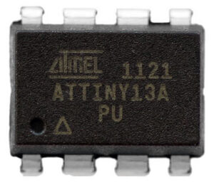
Recovering microcontroller ATtiny13A heximal involves a process of cracking or decoding the secured firmware stored in its flash memory and EEPROM memory of encrypted MCU ATtiny13A. The ATtiny13A, like many microcontrollers (MCUs), may have encrypted or locked firmware to protect its program and source code. However, using reverse engineering techniques, experts can break these ATtiny13A microprocessor’s protective layers and unlock the microprocessor’s memory to retrieve the heximal data.
Recovering microcontroller ATtiny13A heximal involves a process of cracking or decoding the secured firmware stored in its flash memory and EEPROM memory of encrypted MCU ATtiny13A. The ATtiny13A, like many microcontrollers (MCUs), may have encrypted or locked firmware to protect its program and source code. However, using reverse engineering techniques, experts can break these ATtiny13A microprocessor’s protective layers and unlock the microprocessor’s memory to retrieve the heximal data.
The recovery process starts by analyzing the microcontroller’s architecture to identify encryption protocols. Once these protections are bypassed, the binary or heximal firmware can be extracted. This data is essential for restoring or replicating the original program, enabling system recovery or hardware duplication.
Decoding or decrypting the ATtiny13A’s firmware allows developers to restore lost data or replicate the software for new devices. However, these actions must be conducted within legal and ethical guidelines to avoid violating intellectual property rights.
The AVR core combines a rich instruction set with 32 general purpose working registers which will provide benefit for Recover Microcontroller ATtiny13A Heximal. All 32 registers are directly connected to the Arithmetic Logic Unit (ALU), allowing two independent registers to be accessed in one single instruction executed in one clock cycle. The resulting architecture is more code efficient while achieving throughputs up to ten times faster than conventional CISC microcontrollers.
The ATtiny13A provides the following features: 1K byte of In-System Programmable Flash, 64 bytes EEPROM, 64 bytes SRAM, 6 general purpose I/O lines, 32 general purpose working registers, one 8-bit Timer/Counter with compare modes, Internal and External Interrupts, a 4-channel, 10-bit ADC, a programmable Watchdog Timer with internal Oscillator, and three software selectable power saving modes if Recover Microcontroller ATTINY13A Heximal.
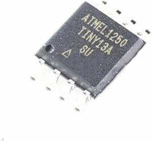
mbalekake microcontroller ATtiny13A heximal melu proses cracking utawa dekoding perangkat kukuh aman disimpen ing memori lampu kilat lan memori EEPROM saka ndhelik MCU ATtiny13A. ATtiny13A, kaya akeh mikrokontroler (MCU), bisa uga duwe perangkat kukuh sing dienkripsi utawa dikunci kanggo nglindhungi program lan kode sumber. Nanging, kanthi nggunakake teknik rekayasa terbalik, para ahli bisa ngilangi lapisan pelindung mikroprosesor ATtiny13A iki lan mbukak kunci memori mikroprosesor kanggo njupuk data heksimal.
The Idle mode stops the CPU while allowing the SRAM, Timer/Counter, ADC, Analog Comparator, and Interrupt system to continue functioning. The Power-down mode saves the register contents, disabling all chip functions until the next Interrupt or Hardware Reset. The ADC Noise Reduction mode stops the CPU and all I/O modules except ADC, to minimize switching noise during ADC conversions.
The device is manufactured using Atmel’s high density non-volatile memory technology. The On-chip ISP Flash allows the Program memory to be re-programmed In-System through an SPI serial interface, by a conventional non-volatile memory programmer or by an On-chip boot code running on the AVR core.
The ATtiny13A AVR is supported with a full suite of program and system development tools including: C Compilers, Macro Assemblers, Program Debugger/Simulators, and Evaluation kits if Recover MICROCONTROLLER.
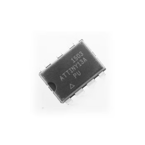
మైక్రోకంట్రోలర్ ATtiny13A హెక్సిమల్ని పునరుద్ధరించడం అనేది దాని ఫ్లాష్ మెమరీలో నిల్వ చేయబడిన సురక్షిత ఫర్మ్వేర్ మరియు ఎన్క్రిప్టెడ్ MCU ATtiny13A యొక్క EEPROM మెమరీని క్రాకింగ్ లేదా డీకోడింగ్ చేసే ప్రక్రియను కలిగి ఉంటుంది. ATtiny13A, అనేక మైక్రోకంట్రోలర్ల (MCUలు) వలె, దాని ప్రోగ్రామ్ మరియు సోర్స్ కోడ్ను రక్షించడానికి ఫర్మ్వేర్ను ఎన్క్రిప్ట్ చేసి లేదా లాక్ చేసి ఉండవచ్చు. అయినప్పటికీ, రివర్స్ ఇంజనీరింగ్ పద్ధతులను ఉపయోగించి, నిపుణులు ఈ ATtiny13A మైక్రోప్రాసెసర్ యొక్క రక్షణ పొరలను విచ్ఛిన్నం చేయవచ్చు మరియు హెక్సిమల్ డేటాను తిరిగి పొందడానికి మైక్రోప్రాసెసర్ మెమరీని అన్లాక్ చేయవచ్చు.
For compatibility with future devices, reserved bits should be written to zero if accessed. Reserved I/O memory addresses should never be written when Break IC PIC16F684 Binary.
I/O Registers within the address range 0x00 – 0x1F are directly bit-accessible using the SBI and CBI instructions. In these registers, the value of single bits can be checked by using the SBIS and SBIC instructions.ome of the Status Flags are cleared by writing a logical one to them. Note that, unlike most other AVRs, the CBI and SBI instructions will only operation the specified bit, and can therefore be used on registers containing such Status Flags. The CBI and SBI instructions work with registers 0x00 to 0x1F.
This documentation contains simple code examples that briefly show how to use various parts of the device. These code examples assume that the part specific header file is included before compilation. Be aware that not all C compiler vendors include bit definitions in the header files and interrupt handling in C is compiler dependent. Please confirm with the C compiler documentation for more details.
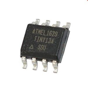
Die Wiederherstellung des Mikrocontrollers ATtiny13A Heximal umfasst einen Prozess zum Knacken oder Dekodieren der gesicherten Firmware, die im Flash-Speicher und EEPROM-Speicher des verschlüsselten MCU ATtiny13A gespeichert ist. Der ATtiny13A kann, wie viele Mikrocontroller (MCUs), eine verschlüsselte oder gesperrte Firmware haben, um sein Programm und seinen Quellcode zu schützen. Mithilfe von Reverse-Engineering-Techniken können Experten jedoch diese Schutzschichten des ATtiny13A-Mikroprozessors durchbrechen und den Speicher des Mikroprozessors entsperren, um die Heximal-Daten abzurufen.
 Recover Microcontroller AT80F51 Eeprom
We can Recover Microcontroller AT80F51 Eeprom, please view the Microcontroller AT80F51 features for your reference:
The AT80F51 is a low-power, high-performance CMOS 8-bit microcomputer with 4K bytes of QuickFlash Memory. The device is manufactured using Atmel’s high density nonvolatile memory technology and is compatible with the industry standard MCS- 51™ instruction set and pinout.
The on-microcontroller QuickFlash allows custom codes to be quickly programmed in the factory. By combining a versatile 8-bit CPU with Quick-Flash on a monolithic microcontroller which carry out the same method as Recover MCU PIC16F876 Binary, the Atmel AT80F51 is a powerful microcomputer which provides a highly flexible and cost effective solution to many embedded control applications.
The AT80F51 provides the following standard features: 4K bytes of QuickFlash, 128 bytes of RAM, 32 I/O lines, two 16-bit timer/counters, a five vector two-level interrupt architecture, a full duplex serial port, on-microcontroller oscillator and clock circuitry. In addition, the AT80F51 is designed with static logic for operation down to zero frequency and supports two software selectable power saving modes through the purpose of Recover MCU PIC16F877 Heximal.
The Idle Mode stops the CPU while allowing the RAM, timer/counters, serial port and interrupt system to continue functioning. The Power Down Mode saves the RAM contents but freezes the oscillator disabling all other microcontroller functions until the next hardware reset.
XTAL1 and XTAL2 are the input and output, respectively, of an inverting amplifier which can be configured for use as an on-microcontroller oscillator, as shown in Figure 1. Either a quartz In idle mode, the CPU puts itself to sleep while all the on- microcontroller peripherals remain active. The mode is invoked by software.
The content of the on-microcontroller RAM and all the special functions registers remain unchanged during this mode. The idle mode can be terminated by any enabled interrupt or by a hardware reset. It should be noted that when idle is terminated by a hardware reset, the device normally resumes program execution when Crack MCU, from where it left off, up to two machine cycles before the internal reset algorithm takes control when Recover Microcontroller AT80F51 Eeprom.
On-microcontroller hardware inhibits access to internal RAM in this event, but access to the port pins is not inhibited. To eliminate the possibility of nated. The only exit from power down is a hardware reset. Reset redefines the SFRs but does not change the on-microcontroller RAM. The reset should not be activated before VCC is restored to its normal operating level and must be held active long enough to allow the oscillator to restart and stabilize.
