Archive for the ‘Recover Chip’ Category
 Restore Microchip PIC18F2550 Memory Data
The OSTS, IOFS and T1RUN bits indicate which clock source is currently providing the device clock. The OSTS bit indicates that the Oscillator Start-up Timer by Restore Microchip PIC18F2550 Memory Data has timed out and the primary clock is providing the device clock in Primary Clock modes.
The IOFS bit indicates when the internal oscillator block has stabi- lized and is providing the device clock in RC Clock modes by Reverse Engineering Encrypted AVR Chip ATtiny261 Software. The T1RUN bit (T1CON<6>) indicates when the Timer1 oscillator is providing the device clock in Secondary Clock modes. In power-managed modes, only one of these three bits will be set at any time. If none of these bits are set, the INTRC is providing the clock or INTOSC has just started and is not yet stable.
The IDLEN bit determines if the device goes into Sleep mode or one of the Idle modes when the SLEEP instruction is executed through Decode Atmel Chip ATtiny461 Encrypted Firmware. The use of the flag and control bits in the OSCCON register is discussed in more detail in Section 3.0 “Power-Managed Modes”.
Note 1: The Timer1 oscillator must be enabled to select the secondary clock source. The Timer1 oscillator is enabled by setting the T1OSCEN bit in the Timer1 Control register (T1CON<3>) in order to Break Encrypted Microprocessor ATtiny861 Embedded Heximal. If the Timer1 oscillator is not enabled, then any attempt to select a secondary clock source will be ignored.
2: It is recommended that the Timer1 oscillator be operating and stable before selecting the secondary clock source or a very long delay may occur while the Timer1 oscillator starts from Restore Microchip PIC18F2550 Memory Data.
PIC18LF2525 devices contain circuitry to prevent clock “glitches” when switching between clock sources. A short pause in the device clock occurs during the clock switch to Crack MCU Program. The length of this pause is the sum of two cycles of the old clock source and three to four cycles of the new clock source for the purpose of Break Atmel MCU ATmega1281 Locked Heximal. This formula assumes that the new clock source is stable. Clock transitions are discussed in greater detail in Section 3.1.2 “Entering Power-Managed Modes”.
 Microprocessor PIC18F2515 Heximal File Recovery
Microprocessor PIC18F2515 heximal file recovery is a process starts from unlock protective PIC18F2515 microchip MCU fuse bit and read embedded firmware out in the format of binary code and heximal data from secured microcontroller PIC18F2515;
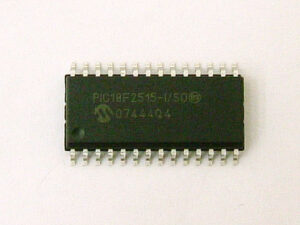
microprocessor PIC18F2515 heximal file recovery is a process starts from unlock protective PIC18F2515 microchip MCU fuse bit and read embedded firmware out in the format of binary code and heximal data from secured microcontroller PIC18F2515;
Using the internal oscillator as the clock source when Crack MCU Flash eliminates the need for up to two external oscillator pins which will provide great benefit for Microprocessor PIC18F2515 Heximal File Recovery and can then be used for digital I/O. Two distinct configurations are available:
- In INTIO1 mode, the OSC2 pin outputs FOSC/4, while OSC1 functions as RA7 for digital input and output.
- In INTIO2 mode, OSC1 functions as RA7 and OSC2 functions as RA6, both for digital input and output.
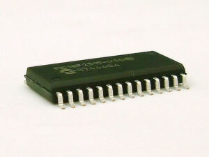
Odzyskiwanie pliku heksadecymalnego mikroprocesora PIC18F2515 to proces rozpoczynający się od odblokowania zabezpieczającego bitu bezpiecznika mikroprocesora PIC18F2515 i odczytania wbudowanego oprogramowania sprzętowego w formacie kodu binarnego i danych heksadecymalnych z zabezpieczonego mikrokontrolera PIC18F2515;
The internal oscillator block is calibrated at the factory to produce an INTOSC output frequency of 8.0 MHz through the process of Restore Microprocessor Program Most Important Two Steps. The INTRC oscillator operates independently of the INTOSC source. Any changes in INTOSC across voltage and temperature are not necessarily reflected by changes in INTRC and vice versa.
The internal oscillator’s output has been calibrated at the factory but can be adjusted in the user’s application. This is done by writing to the OSCTUNE register (Register 2-1).
When the OSCTUNE register is modified, the INTOSC frequency will begin shifting to the new frequency. The INTOSC clock will stabilize within 1 ms by Break Atmel AVR MCU ATmega8535L Heximal. Code execution continues during this shift. There is no indication that the shift has occurred.
The OSCTUNE register also implements the INTSRC and PLLEN bits, which control certain features of the internal oscillator block. The INTSRC bit allows users to select which internal oscillator provides the clock source when the 31 kHz frequency option is selected for the purpose of Microprocessor PIC18F2515 Heximal File Recovery. This is covered in greater detail in Section 2.7.1 “Oscillator Control Register”.
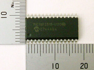
mikroişlemci PIC18F2515 heksimal dosya kurtarma işlemi, koruyucu PIC18F2515 mikroçip MCU sigorta bitinin kilidini açmak ve güvenli mikrodenetleyici PIC18F2515’ten ikili kod ve heksimal veri biçiminde gömülü aygıt yazılımını okumakla başlayan bir işlemdir;
The PLLEN bit controls the operation of the frequency multiplier, PLL, in Internal Oscillator modes after Recover Atmel AVR Controller ATmega48V Firmware.
The 4x frequency multiplier can be used with the internal oscillator block to produce faster device clock speeds than are normally possible with an internal oscillator. When enabled, the PLL produces a clock speed of up to 32 MHz. Unlike HSPLL mode, the PLL is controlled through software. The control bit, PLLEN (OSCTUNE<6>), is used to enable or disable its operation by Break IC ATmega88V Internal Flash.
The PLL is available for use with the INTOSC when:
- The primary clock is the INTOSC clock source (selected in CONFIG1H<3:0>), and
- The 4 or 8 MHz INTOSC output is selected.
Writes to the PLLEN bit will be ignored until both these conditions are met.
 Losted PIC18F2458 Microcontroller Embedded Code Restoration
Losted PIC18F2458 microcontroller embedded code restoration is a process to recover binary file or heximal data from PIC18F2458 protective MICROCHIP MCU flash memory and eeprom memory, through PIC18F2458 microprocessor fuse bit unlocking technique;
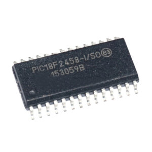
losted PIC18F2458 microcontroller embedded code restoration is a process to recover binary file or heximal data from PIC18F2458 protective MICROCHIP MCU flash memory and eeprom memory, through PIC18F2458 microprocessor fuse bit unlock technique;
Without the back-up embedded firmware from microcontrollers sometimes could become the disaster for a company which try to rescue the obselete or not-produce-anymore devices, through our techniques, Losted PIC18F2458 Microcontroller Embedded Code Restoration process will help you get the firmware back from original PIC18F2458:
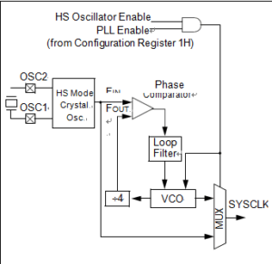
The HSPLL mode makes use of the HS mode oscillator for frequencies up to 10 MHz. A PLL then multiplies the oscillator output frequency by 4 to produce an internal clock frequency up to 40 MHz. The PLLEN bit is not available in this oscillator mode before Microchip PIC18F2520 Embedded Firmware Extraction.
Восстановление встроенного кода потерянного микроконтроллера PIC18F2458 представляет собой процесс восстановления двоичного файла или шестнадцатеричных данных из защитной флэш-памяти микроконтроллера MICROCHIP PIC18F2458 и памяти EEPROM с помощью техники разблокировки бита предохранителя микропроцессора PIC18F2458;
The PLL is only available to the crystal oscillator when the FOSC3:FOSC0 Configuration bits are programmed for HSPLL mode (= 0110).
The PLL is also available to the internal oscillator block when the INTOSC is configured as the primary clock source from Microchip MCU PIC16F870 Heximal Code Restoration. In this configuration, the PLL is enabled in soft- ware and generates a clock output of up to 32 MHz.
The PIC18LF2458 devices include an internal oscillator block which generates two different clock signals; either can be used as the micro- controller’s clock source. This may eliminate the need for external oscillator circuits on the OSC1 and/or OSC2 pins in order to Recover Freescale MCU MC9S12XDG128 Memory Program.
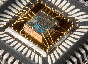
kaybolan PIC18F2458 mikrodenetleyici gömülü kod restorasyonu, PIC18F2458 koruyucu MICROCHIP MCU flaş belleğinden ve eeprom belleğinden, PIC18F2458 mikroişlemci sigorta biti kilit açma tekniği aracılığıyla ikili dosya veya onaltılık verileri kurtarmak için bir işlemdir;
The main output (INTOSC) is an 8 MHz clock source, which can be used to directly drive the device clock. It also drives a postscaler, which can provide a range of clock frequencies from 31 kHz to 4 MHz. The INTOSC output is enabled when a clock frequency from 125 kHz to 8 MHz is selected, and can provide 31 kHz if required.
The other clock source is the internal RC oscillator (INTRC) which provides a nominal 31 kHz output after Reverse Engineering Microchip PIC16F1913 Memory. INTRC is enabled if it is selected as the device clock source; it is also enabled automatically when any of the following are enabled:
• Power-up Timer
• Fail-Safe Clock Monitor
• Watchdog Timer
These features are discussed in greater detail in Section 23.0 “Special Features of the CPU”.
The clock source frequency (INTOSC direct, INTRC direct or INTOSC postscaler) is selected by configuring the IRCF bits of the OSCCON register before Unlock Microcontroller Flash. Additionally, the 31 kHz clock can be provided by either the INTOSC, or INTRC clock sources, depending on the INTSRC bit (OSCTUNE<7>).
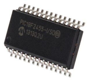
 Recover Microchip PIC18F2455 Memory Program
Recover Microchip MCU PIC18F2455 memory program starts from crack encrypted microcontroller PIC18F2455 tamper resistance and then readout embedded firmware from locked microprocessor PIC18F2455 in the format of binary data or heximal file;
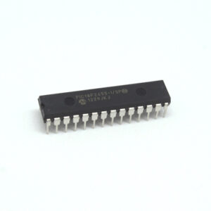
recover Microchip MCU PIC18F2455 memory program starts from crack encrypted microcontroller PIC18F2455 tamper resistance and then readout embedded firmware from locked microprocessor PIC18F2455 in the format of binary data or heximal file;
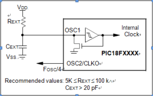
As one of the most important components to Recover Microchip PIC18F2455 Memory Program, for timing insensitive applications, the “RC” and “RCIO” device options offer additional cost savings. The actual oscillator frequency is a function of several factors:
• supply voltage
• values of the external resistor (REXT) and capacitor (CEXT)
• operating temperature
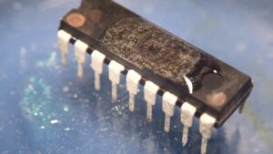
يبدأ برنامج استعادة ذاكرة Microchip MCU PIC18F2455 من كسر مقاومة العبث بالميكروكنترولر المشفر PIC18F2455 ثم قراءة البرامج الثابتة المضمنة من المعالج الدقيق المقفل PIC18F2455 بتنسيق بيانات ثنائية أو ملف سداسي عشري؛
Given the same device, operating voltage and temperature and component values, there will also be unit-to-unit frequency variations before Recover PIC MCU Microchip PIC16LF506 Firmware. These are due to factors such as:
• normal manufacturing variation
• difference in lead frame capacitance between package types (especially for low CEXT values)
• variations within the tolerance of limits of REXT and CEXT
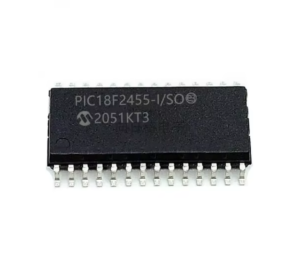
Программа восстановления памяти микроконтроллера Microchip PIC18F2455 запускается с взломанного зашифрованного микроконтроллера PIC18F2455, защищенного от несанкционированного доступа, а затем считывает встроенную прошивку с заблокированного микропроцессора PIC18F2455 в формате двоичных данных или шестнадцатеричного файла;
In the RC Oscillator mode, the oscillator frequency divided by 4 is available on the OSC2 pin when Decrypt Microchip PIC18F2321 MCU Heximal File. This signal may be used for test purposes or to synchronize other logic after Recover PIC MCU Microchip 12F510 Firmware. Below Figure shows how the R/C combination is connected.
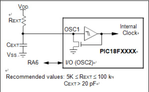
The RCIO Oscillator mode (below Figure) functions like the RC mode, except that the OSC2 pin becomes an additional general purpose I/O pin. The I/O pin becomes bit 6 of PORTA (RA6).
A Phase Locked Loop (PLL) circuit is provided as an option for users who wish to use a lower frequency oscillator circuit, or to clock the device up to its highest rated frequency from a crystal oscillator after Copy Encrypted Microchip PIC18F2330 Heximal. This may be useful for customers who are concerned with EMI due to high-frequency crystals, or users who require higher clock speeds from an internal oscillator if the Microcontroller unlocking is completed.
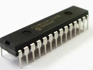
 Recover PIC18F2431 MCU Locked Program
Recover PIC18F2431 MCU locked program needs to unlock encrypted microcontroller PIC18F2431 tamper resistance system, and extract embedded firmware also known as source code from secured microprocessor PIC18F2431 flash binary file memory or eeprom heximal data memory;
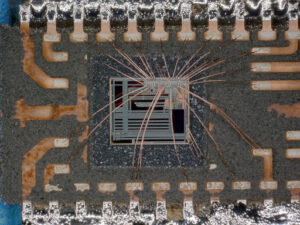
recover PIC18F2431 MCU locked program needs to unlock encrypted microcontroller PIC18F2431 tamper resistance system, and extract embedded firmware also known as source code from secured microprocessor PIC18F2431 flash binary file memory or eeprom heximal data memory
Besides its availability as a clock source when Microchip PIC18F2520 Embedded Firmware Extraction, the internal oscillator block provides a stable reference source that gives the family additional features for robust operation and hacker can technically Recover PIC18F2431 MCU Locked Program through power glitch on it:
- Fail-Safe Clock Monitor: This option constantly monitors the main clock source against a reference signal provided by the internal oscillator. If a clock failure occurs, the controller is switched to the internal oscillator block after Microchip MCU PIC16F870 Heximal Code Restoration, allowing for continued operation or a safe application shutdown.
Two-Speed Start-up: This option allows the internal oscillator to serve as the clock source from Power-on Reset, or wake-up from Sleep mode, until the primary clock source is available.
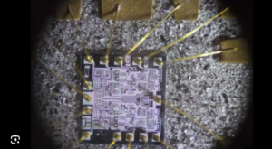
بازیابی PIC18F2431 برنامه قفل شده MCU باید سیستم مقاومت در برابر دستکاری میکروکنترلر رمزگذاری شده PIC18F2431 را باز کند و سیستم عامل تعبیه شده را که به عنوان کد منبع شناخته می شود از حافظه فایل باینری فلش ریزپردازنده ایمن PIC18F2431 یا حافظه داده هگزیمال eeprom استخراج کند.
- 12-Bit A/D Converter: This module incorporates programmable acquisition time, allowing for a channel to be selected and a conversion to be initiated without waiting for a sampling period and thus, reducing code overhead.
- Memory Endurance: The Enhanced Flash cells for both program memory and data EEPROM are rated to last for many thousands of erase/write cycles – up to 100,000 for program memory and 1,000,000 for EEPROM by Recover Freescale MCU MC9S12XDG128 Memory Program. Data retention without refresh is conservatively estimated to be greater than 40 years.
- Self-Programmability: These devices can write to their own program memory spaces under inter- nal software control. By using a bootloader routine located in the protected Boot Block at the top of program memory, it becomes possible to create an application that can update itself in the field.
- Extended Instruction Set: Recover PIC18F2431 MCU Locked Program introduces an optional extension to the PIC18 instruction set, which adds eight new instructions and an Indexed Addressing mode. This extension, enabled as a device con- figuration option, has been specifically designed to optimize re-entrant application code originally developed in high-level languages, such as C.
PIC18F2431 MCU लॉक किए गए प्रोग्राम को पुनर्प्राप्त करने के लिए एन्क्रिप्टेड माइक्रोकंट्रोलर PIC18F2431 छेड़छाड़ प्रतिरोध प्रणाली को अनलॉक करने की आवश्यकता है, और सुरक्षित माइक्रोप्रोसेसर PIC18F2431 फ्लैश बाइनरी फ़ाइल मेमोरी या ईप्रोम हेक्सिमल डेटा मेमोरी से एम्बेडेड फर्मवेयर को निकालने की आवश्यकता है जिसे स्रोत कोड के रूप में भी जाना जाता है
- Enhanced CCP module: In PWM mode, this module provides 1, 2 or 4 modulated outputs for controlling half-bridge and full-bridge drivers. Other features include auto-shutdown, for disabling PWM outputs on interrupt or other select conditions and auto-restart after Reverse Engineering Microchip PIC16F1913 Memory, to reactivate outputs once the condition has cleared.
- Enhanced Addressable USART: This serial communication module is capable of standard.
RS-232 operation and provides support for the LIN bus protocol. Other enhancements include automatic baud rate detection and a 16-bit Baud Rate Generator for improved resolution. When the microcontroller is using the internal oscillator block to Clone IC Code, the EUSART provides stable operation for applications that talk to the outside world without using an external crystal (or its accompanying power requirement).
- Extended Watchdog Timer (WDT): This enhanced version incorporates a 16-bit prescaler, allowing an extended time-out range that is stable across operating voltage and temperature.

recuperar o programa bloqueado do MCU PIC18F2431 precisa desbloquear o sistema de resistência à violação do microcontrolador PIC18F2431 criptografado e extrair o firmware incorporado, também conhecido como código-fonte, da memória de arquivo binário flash do microprocessador PIC18F2431 protegido ou da memória de dados hexadecimal eeprom
 Recover Microprocessor ATMEGA640V Firmware
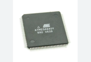
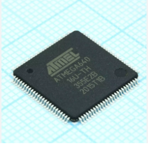
Recovering Microprocessor ATMEGA640V firmware is a highly technical process that often involves reverse engineering techniques to crack and decrypt the protected code stored within the microcontroller. The firmware, which operates at the core of the microprocessor’s functionality, is typically encoded in binary or hexadecimal (hex) format. To recover the ATMEGA640V firmware, engineers may need to decode this complex data and understand its structure, enabling them to copy and restore the original functions of the device.
Възстановяване на фърмуера на микропроцесор ATMEGA640V е изключително технически процес, който често включва техники за обратно инженерство за кракване и дешифриране на защитения код, съхраняван в микроконтролера. Фърмуерът, който работи в основата на функционалността на микропроцесора ATMEGA640V, обикновено е кодиран в двоичен или шестнадесетичен (шестнадесетичен) формат. За да възстановят фърмуера на ATMEGA640V, инженерите може да се наложи да декодират тези сложни данни и да разберат структурата им, което им позволява да копират и възстановят оригиналните функции на устройството.
In many cases, firmware recovery requires cracking the security features of the microcontroller (MCU), which are designed to prevent unauthorized access. This can involve analyzing the microprocessor’s internal architecture, exploiting vulnerabilities, or using specialized equipment to bypass encryption. Once decrypted, the binary or hex representation of the firmware can be decoded and reassembled for restoration or analysis.
We can recover microprocessor ATMEGA640V firmware, please view the microprocessor ATMEGA640V features for your reference:
XTAL1 and XTAL2 are the input and output, respectively, of an inverting amplifier that can be configured for use as an on-chip oscillator by Copy Microcontroller PIC12F675 Firmware. Either a quartz crystal or ceramic resonator may be used.
To drive the device from an external clock source, XTAL2 should be left unconnected while XTAL1 is driven, as shown in Figure 12.
There are no requirements on the duty cycle of the external clock signal, since the input to the internal clocking circuitry is through a divide-by-two flip-flop, but minimum and maximum voltage high and low time specifications must be observed if Recover Microprocessor ATmega640V Firmware.
माइक्रोप्रोसेसर ATMEGA640V फर्मवेयर को पुनर्प्राप्त करना एक अत्यधिक तकनीकी प्रक्रिया है जिसमें अक्सर माइक्रोकंट्रोलर के भीतर संग्रहीत संरक्षित कोड को क्रैक और डिक्रिप्ट करने के लिए रिवर्स इंजीनियरिंग तकनीक शामिल होती है। ATMEGA640V माइक्रोप्रोसेसर की कार्यक्षमता के मूल में संचालित होने वाला फर्मवेयर आमतौर पर बाइनरी या हेक्साडेसिमल (हेक्स) प्रारूप में एन्कोड किया जाता है। ATMEGA640V फर्मवेयर को पुनर्प्राप्त करने के लिए, इंजीनियरों को इस जटिल डेटा को डिकोड करने और इसकी संरचना को समझने की आवश्यकता हो सकती है, जिससे वे डिवाइस के मूल कार्यों को कॉपी और पुनर्स्थापित कर सकें।
In idle mode, the CPU puts itself to sleep while all the on-chip peripherals remain active in the process of Copy MCU PIC18F4685 Software. The mode is invoked by software. The content of the on-chip RAM and all the special functions registers remain unchanged during this mode. The idle mode can be terminated by any enabled interrupt or by a hardware reset.
Note that when idle mode is terminated by a hardware reset, the device normally resumes firmware execution from where it left off, up to two machine cycles before the internal reset algorithm takes control. On-chip hardware inhibits access to internal RAM in this event by Unlock Microcontroller Firmware, but access to the port pins is not inhibited.
To eliminate the possibility of an unexpected write to a port pin when idle mode is terminated by a reset for support the progress of Copy IC PIC18F458 Binary, the instruction following the one that invokes idle mode should not write to a port pin or to external memory.
بازیابی سیستم عامل میکروپروسسور ATMEGA640V یک فرآیند بسیار فنی است که اغلب شامل تکنیک های مهندسی معکوس برای شکستن و رمزگشایی کد محافظت شده ذخیره شده در میکروکنترلر است. سفتافزار، که در هسته عملکرد ریزپردازنده ATMEGA640V کار میکند، معمولاً در قالب باینری یا هگزا دسیمال (هگز) کدگذاری میشود. برای بازیابی سفتافزار ATMEGA640V، مهندسان ممکن است نیاز به رمزگشایی این دادههای پیچیده و درک ساختار آن داشته باشند و آنها را قادر میسازد تا عملکردهای اصلی دستگاه را کپی و بازیابی کنند.
In the power down mode, the oscillator is stopped and the instruction that invokes power down is the last instruction executed. The on-chip RAM and Special Function Registers retain their values until the power down mode is terminated.
Exit from power down can be initiated either by a hardware reset or by an enabled external interrupt. Reset redefines the SFRs but does not change the on-chip RAM. The reset should not be activated before VCC is restored to its normal operating level and must be held active long enough to allow the oscillator to restart and stabilize before Recover Chip MC9S08DZ32ACLC Firmware.
To exit power down via an interrupt, the external interrupt must be enabled as level sensitive before entering power down. The interrupt service routine starts at 16 ms (nominal) after the enabled interrupt pin is activated.
 Recover MCU ATMEGA162A Heximal
Recovering MCU ATMEGA162A heximal data is a meticulous process involving advanced techniques to decode and restore the embedded firmware stored within this microcontroller’s flash memory program. This task may arise when source code or program data becomes corrupted, lost, or requires duplication for compatible systems. The ATMEGA162A MCU, known for its reliability in embedded applications, stores critical information in binary format within its EEPROM and flash memory.
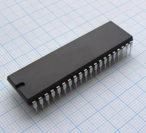
recovering MCU ATMEGA162A heximal data is a meticulous process involving advanced techniques to decode and restore the embedded firmware stored within this microcontroller’s flash memory program. This task may arise when source code or program data becomes corrupted, lost, or requires duplication for compatible systems. The ATMEGA162A MCU, known for its reliability in embedded applications, stores critical information in binary format within its EEPROM and flash memory
To recover the heximal file, reverse engineering tools are often used to break the security layers protecting the firmware. This process involves decoding the binary data and converting it into a heximal file that represents the original source code. By reconstructing the code, engineers can clone or duplicate the program for testing, troubleshooting, or system recovery purposes. However, any attempt to access EEPROM memory data must be done cautiously to avoid corrupting the firmware, as the ATMEGA162A’s security features are designed to prevent unauthorized access.
Successfully recovering MCU ATMEGA162A heximal data allows for precise replication of the original firmware, enabling continued use or adaptation of the program across various hardware setups. This approach is essential for maintaining system reliability and ensuring compatibility in embedded applications.
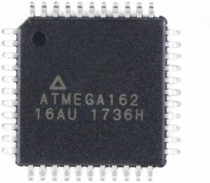
بازیابی دادههای هگزیمال MCU ATMEGA162A یک فرآیند دقیق شامل تکنیکهای پیشرفته برای رمزگشایی و بازیابی میانافزار تعبیهشده ذخیرهشده در برنامه حافظه فلش این میکروکنترلر است. این کار ممکن است زمانی ایجاد شود که کد منبع یا داده های برنامه خراب شود، از بین برود یا برای سیستم های سازگار نیاز به تکرار داشته باشد. ATMEGA162A MCU، که به خاطر قابلیت اطمینان خود در برنامه های جاسازی شده معروف است، اطلاعات حیاتی را در قالب باینری در EEPROM و حافظه فلش خود ذخیره می کند.
When the SM2..0 bits are 111 and an external crystal/resonator clock option is selected, the SLEEP instruction makes the MCU Cracking enter Extended Standby mode. This mode is identical to Power-save mode with the exception that the Oscillator is kept running.
From Extended Standby mode, the device wakes up in six clock cycles. The Power Reduction Register, PRR, provides a method to stop the clock to individual peripherals to reduce power consumption. The current state of the peripheral is frozen and the I/O registers can not be read or written in the process of Recover MCU heximal.
Resources used by the peripheral when stopping the clock will remain occupied, hence the peripheral should in most cases be disabled before stopping the clock. Waking up a module, which is done by clearing the bit in PRR, puts the module in the same state as before shutdown.
Module shutdown can be used in Idle mode and Active mode to significantly reduce the overall power consumption. See “Supply Current of IO modules” on page 381 for examples. In all other sleep modes, the clock is already stopped.
Bit 7 – PRTWI: Power Reduction TWI
Writing a logic one to this bit shuts down the TWI by stopping the clock to the module. When waking up the TWI again, the TWI should be re initialized to ensure proper operation when recover MCU heximal.
Bit 6 – PRTIM2: Power Reduction Timer/Counter2
Writing a logic one to this bit shuts down the Timer/Counter2 module in synchronous mode (AS2 is 0). When the Timer/Counter2 is enabled, operation will continue like before the shutdown.
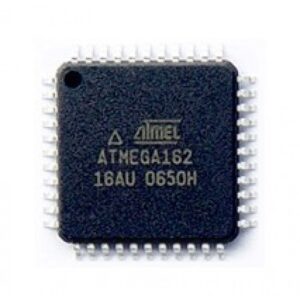
Die Wiederherstellung von MCU ATMEGA162A-Heximaldaten ist ein sorgfältiger Prozess, der fortschrittliche Techniken zum Dekodieren und Wiederherstellen der eingebetteten Firmware umfasst, die im Flash-Speicherprogramm dieses Mikrocontrollers gespeichert ist. Diese Aufgabe kann auftreten, wenn Quellcode oder Programmdaten beschädigt werden oder verloren gehen oder für kompatible Systeme dupliziert werden müssen. Die ATMEGA162A-MCU, die für ihre Zuverlässigkeit in eingebetteten Anwendungen bekannt ist, speichert kritische Informationen im Binärformat in ihrem EEPROM und Flash-Speicher.
Bit 5 – PRTIM0: Power Reduction Timer/Counter0
Writing a logic one to this bit shuts down the Timer/Counter0 module. When the Timer/Counter0 is enabled, operation will continue like before the shutdown.
Bit 4 – Res: Reserved bit
This bit is reserved bit and will always read as zero.
Bit 3 – PRTIM1: Power Reduction Timer/Counter1
Writing a logic one to this bit shuts down the Timer/Counter1 module. When the Timer/Counter1 is enabled, operation will continue like before the shutdown.
Bit 2 – PRSPI: Power Reduction Serial Peripheral Interface
Writing a logic one to this bit shuts down the Serial Peripheral Interface by stopping the clock to the module. When waking up the SPI again, the SPI should be re initialized to ensure proper operation after Break Chip Atmel Atmega48PV Heximal.
Bit 1 – PRUSART0: Power Reduction USART0
Writing a logic one to this bit shuts down the USART0 by stopping the clock to the module. When waking up the USART0 again, the USART0 should be re initialized to ensure proper operation.
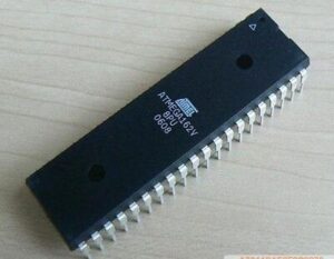
MCU ATMEGA162A हेक्सिमल डेटा को पुनर्प्राप्त करना एक सावधानीपूर्वक प्रक्रिया है जिसमें इस माइक्रोकंट्रोलर के फ्लैश मेमोरी प्रोग्राम में संग्रहीत एम्बेडेड फ़र्मवेयर को डिकोड और पुनर्स्थापित करने के लिए उन्नत तकनीकें शामिल हैं। यह कार्य तब हो सकता है जब स्रोत कोड या प्रोग्राम डेटा दूषित हो जाता है, खो जाता है, या संगत सिस्टम के लिए दोहराव की आवश्यकता होती है। ATMEGA162A MCU, एम्बेडेड अनुप्रयोगों में अपनी विश्वसनीयता के लिए जाना जाता है, अपने EEPROM और फ्लैश मेमोरी के भीतर बाइनरी प्रारूप में महत्वपूर्ण जानकारी संग्रहीत करता है
 Recover MCU ATTINY25 Flash
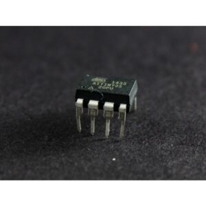
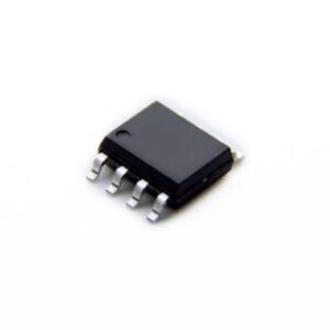
Recovering MCU ATTINY25 flash memory involves advanced techniques to crack or decrypt its secured and encrypted firmware. This protective microcomputer is designed with robust security features, making access to its locked flash memory and EEPROM memory a challenging task. Reverse engineering plays a vital role in understanding the microcontroller’s architecture and identifying vulnerabilities that can be exploited to break its protective mechanisms.
Việc khôi phục bộ nhớ flash MCU ATTINY25 liên quan đến các kỹ thuật tiên tiến để bẻ khóa hoặc giải mã chương trình cơ sở được mã hóa và bảo mật của nó. Máy vi tính bảo vệ này được thiết kế với các tính năng bảo mật mạnh mẽ, khiến việc truy cập vào bộ nhớ flash bị khóa và bộ nhớ EEPROM của nó trở thành một nhiệm vụ đầy thách thức. Kỹ thuật đảo ngược đóng vai trò quan trọng trong việc hiểu kiến trúc của bộ vi điều khiển và xác định các lỗ hổng có thể bị khai thác để phá vỡ các cơ chế bảo vệ của nó.
The recovery process often requires specialized hardware and software tools to extract the binary or heximal data stored in the MCU’s memory. By attacking the encrypted security layers, it becomes possible to retrieve the embedded program and source code for restoration or cloning. This can be crucial for system diagnostics, program replication, or firmware backups.
Once the flash memory is successfully accessed, the extracted firmware can be restored to its original functionality or cloned for use in duplicate systems. This process ensures the continuity of operations in cases of hardware failure or program corruption. However, handling such secured microprocessors requires a high level of technical expertise and strict adherence to ethical and legal standards. Unauthorized access to the ATTINY25’s flash memory or software may violate intellectual property rights, emphasizing the importance of responsible and authorized recovery practices.
MCU ATTINY25 फ्लैश मेमोरी को रिकवर करने के लिए इसके सुरक्षित और एन्क्रिप्टेड फर्मवेयर को क्रैक या डिक्रिप्ट करने के लिए उन्नत तकनीकों की आवश्यकता होती है। इस सुरक्षात्मक माइक्रोकंप्यूटर को मजबूत सुरक्षा सुविधाओं के साथ डिज़ाइन किया गया है, जिससे इसकी लॉक की गई फ्लैश मेमोरी और EEPROM मेमोरी तक पहुँचना एक चुनौतीपूर्ण कार्य बन जाता है। रिवर्स इंजीनियरिंग माइक्रोकंट्रोलर की वास्तुकला को समझने और उन कमजोरियों की पहचान करने में महत्वपूर्ण भूमिका निभाती है जिनका उपयोग इसके सुरक्षात्मक तंत्र को तोड़ने के लिए किया जा सकता है।
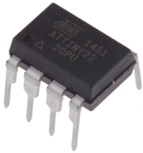
The ATtiny25 is a low-power CMOS 8-bit mcu based on the AVR enhanced RISC architecture. By executing powerful instructions in a single clock cycle, the ATtiny25 achieves throughputs approaching 1 MIPS per MHz allowing the system designer to optimize power consumption versus processing speed when Recover MCU ATTINY25 Flash.
The AVR core combines a rich instruction set with 32 general purpose working registers. All the 32 registers are directly connected to the Arithmetic Logic Unit (ALU) for the purpose of Copy Microcontroller PIC16F737 Flash, allowing two independent registers to be accessed in one single instruction executed in one clock cycle.
The resulting architecture is more code efficient while achieving throughputs up to ten times faster than conventional CISC mcus.
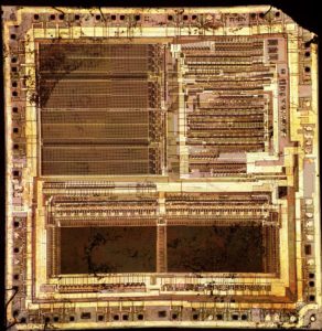
Recover MCU ATTINY25 Flash
The ATtiny25 provides the following features: 2/4/8K byte of In-System Programmable Flash, 128/256/512 bytes EEPROM, 128/256/256 bytes SRAM, 6 general purpose I/O lines, 32 general purpose working registers, one 8-bit Timer/Counter with compare modes, one 8-bit high speed Timer/Counter, Universal Serial Interface, Internal and External Interrupts, a 4-channel, 10-bit ADC, a programmable Watchdog Timer with internal Oscillator, and three software selectable power saving modes which will facilitate the process of Break Chip PIC16F785 Heximal.
The Idle mode stops the CPU while allowing the SRAM, Timer/Counter, ADC, Analog Comparator, and Interrupt system to continue functioning. The Power-down mode saves the register contents, disabling all chip functions until the next Interrupt or Hardware Reset.
The ADC Noise Reduction mode stops the CPU and all I/O modules except ADC, to minimize switching noise during ADC conversions. The device is manufactured using Atmel’s high density non-volatile memory MCU Crack technology. The On-chip ISP Flash allows the Program memory to be re-programmed In-System through an SPI serial interface after Attack MCU PIC16F636 Binary, by a conventional non-volatile memory programmer or by an On-chip boot code running on the AVR core.
การกู้คืนหน่วยความจำแฟลช MCU ATTINY25 ต้องใช้เทคนิคขั้นสูงในการแคร็กหรือถอดรหัสเฟิร์มแวร์ที่ได้รับการรักษาความปลอดภัยและเข้ารหัส ไมโครคอมพิวเตอร์ป้องกันนี้ได้รับการออกแบบด้วยคุณสมบัติความปลอดภัยที่แข็งแกร่ง ทำให้การเข้าถึงหน่วยความจำแฟลชที่ถูกล็อคและหน่วยความจำ EEPROM เป็นงานที่ท้าทาย วิศวกรรมย้อนกลับมีบทบาทสำคัญในการทำความเข้าใจสถาปัตยกรรมของไมโครคอนโทรลเลอร์และระบุช่องโหว่ที่อาจถูกใช้ประโยชน์เพื่อทำลายกลไกการป้องกัน
The ATtiny25 AVR is supported with a full suite of program and system development tools including: C Compilers, Macro Assemblers, Program Debugger/Simulators, In-Circuit Emulators, and Evaluation kits.
 Recover Microcontroller Attiny44 Code
Recovering Microcontroller ATTINY44 code involves advanced techniques to crack and decode its secured and encrypted firmware. This protective microcomputer is designed with robust security features that lock access to its software, source code, and EEPROM memory. Reverse engineering is often required to break through these protective measures, enabling access to the binary or heximal data stored within the MCU.
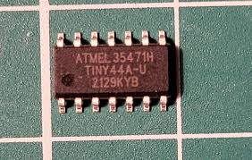
восстановление кода микроконтроллера ATtiny44 включает в себя передовые методы взлома и декодирования его защищенной и зашифрованной прошивки. Этот защитный микрокомпьютер ATtiny44 разработан с надежными функциями безопасности, которые блокируют доступ к его программному обеспечению, исходному коду и памяти EEPROM. Обратное проектирование часто требуется для взлома этих защитных мер, что позволяет получить доступ к двоичным или шестнадцатеричным данным, хранящимся в микроконтроллере ATtiny44.
The process starts by analyzing the microcontroller’s architecture to unlock its firmware and retrieve the embedded program. Specialized tools are used to decode the secured layers, ensuring the integrity of the recovered code. Once the source code is restored, it can be cloned for legitimate purposes such as hardware replication, software backups, or system diagnostics.
Unlocking a locked microprocessor like the ATTINY44 demands precision and adherence to ethical and legal guidelines, ensuring that recovering, restoring, or cloning its firmware serves authorized and constructive objectives.
We can Recover MCU ATTINY44 Code, please view the MICROCONTROLLER ATTINY44 features for your reference:
EEPROM read from application code does not work in Lock Bit Mode 3
Reading EEPROM when system clock frequency is below 900 kHz may not work, EEPROM read from application code does not work in Lock Bit Mode 3 When the Memory Lock Bits LB2 and LB1 are programmed to mode 3 in order to Attack IC PIC16C74B Binary, EEPROM read does not work from the application code from MCU Cracking. Problem Fix/Work around Do not set Lock Bit Protection Mode 3 when the application code needs to read from EEPROM.
Reading EEPROM when system clock frequency is below 900 kHz may not work Reading data from the EEPROM at system clock frequency below 900 kHz may result in wrong data read. Problem Fix/Work around Avoid using the EEPROM at clock frequency below 900 kHz before Recover Microcontroller Attiny44 Code. Reading EEPROM when system clock frequency is below 900 kHz may not work
Reading EEPROM when system clock frequency is below 900 kHz may not work Reading data from the EEPROM at system clock frequency below 900 kHz may result in wrong data read.
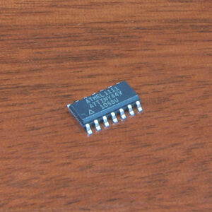
recuperar o código do microcontrolador ATtiny44 envolve técnicas avançadas para quebrar e decodificar seu firmware protegido e criptografado. Este microcomputador protetor ATtiny44 é projetado com recursos de segurança robustos que bloqueiam o acesso ao seu software, código-fonte e memória EEPROM. A engenharia reversa é frequentemente necessária para romper essas medidas de proteção, permitindo o acesso aos dados binários ou hexagonais armazenados dentro do MCU ATtiny44.
Problem Fix/Work around Avoid using the EEPROM at clock frequency below 900 kHz.
Port A is a 8-bit bi-directional I/O port with internal pull-up resistors (selected for each bit). The Port A output buffers have symmetrical drive characteristics with both high sink and source capability. As inputs, Port A pins that are externally pulled low will source current if the pull-up resistors are activated for the purpose of Copy IC PIC12C671 Eeprom. The Port A pins are tri-stated when a reset condition becomes active, even if the clock is not running.
Port A has an alternate functions as analog inputs for the ADC, analog comparator, timer/counter, SPI and pin change interrupt as described in ”Alternate Port Functions”. Port B is a 4-bit bi-directional I/O port with internal pull-up resistors (selected for each bit). The Port B output buffers have symmetrical drive characteristics with both high sink and source capability except PB3 which has the RESET capability to support the process of Copy IC PIC16F884 Code.
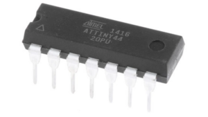
تتضمن استعادة شفرة المتحكم الدقيق ATtiny44 تقنيات متقدمة لكسر وفك تشفير البرامج الثابتة المؤمنة والمشفرة. تم تصميم هذا المتحكم الدقيق ATtiny44 الواقي بميزات أمان قوية تغلق الوصول إلى برمجياته ورمزه المصدري وذاكرة EEPROM. غالبًا ما تكون الهندسة العكسية مطلوبة لاختراق هذه التدابير الوقائية، مما يتيح الوصول إلى البيانات الثنائية أو السداسية المخزنة داخل وحدة التحكم الدقيقة ATtiny44.
To use pin PB3 as an I/O pin, instead of RESET pin, program (‘0’) RSTDISBL fuse. As inputs, Port B pins that are externally pulled low will source current if the pull-up resistors are activated. The Port B pins are tri-stated when a reset condition becomes active, even if the clock is not running. Port B also serves the functions of various special features of the ATtiny24/44/84 as listed on Section 12.3 ”Alternate Port Functions” on page 61.
 Recover IC ATMEGA168PA Program
Recovering IC ATMEGA168PA program often requires expertise in cracking or decoding its encrypted firmware to access the locked content stored within this secured microcontroller. The ATMEGA168PA, a protective microcomputer, is designed to safeguard its EEPROM memory, firmware, and binary data, ensuring that its program and source code remain protected from unauthorized access. Reverse engineering plays a pivotal role in unlocking its protective mechanisms, allowing professionals to analyze and extract the embedded software.
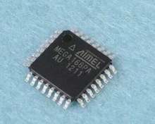
Recovering IC ATMEGA168PA program often requires expertise in cracking or decoding its encrypted firmware to access the locked content stored within this secured microcontroller. The ATMEGA168PA, a protective microcomputer, is designed to safeguard its EEPROM memory, firmware, and binary data, ensuring that its program and source code remain protected from unauthorized access. Reverse engineering plays a pivotal role in unlocking its protective mechanisms, allowing professionals to analyze and extract the embedded software.
The process typically involves identifying the microcontroller’s encryption layers and using specialized tools to break or bypass its security measures. By decoding the binary or heximal structure of the program, the locked firmware can be accessed and restored for authorized purposes. This may include cloning the firmware to replicate hardware, creating backups, or performing system diagnostics to resolve operational issues.
Unlocking and recovering the program from the IC ATMEGA168PA enables developers to restore lost or corrupted source code, ensuring continued functionality of critical systems. Cloning the secured microprocessor can also provide a reliable backup for future use, safeguarding against potential data loss.
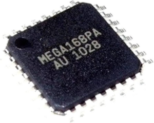
восстановление программы IC ATmega168PA часто требует экспертных знаний по взлому или декодированию ее зашифрованной прошивки для доступа к заблокированному содержимому, хранящемуся в этом защищенном микроконтроллере ATmega168PA. ATMEGA168PA, защитный микрокомпьютер ATmega168PA, разработан для защиты своей памяти EEPROM, прошивки и двоичных данных, гарантируя, что его программа и исходный код остаются защищенными от несанкционированного доступа. Обратное проектирование играет ключевую роль в разблокировке его защитных механизмов, позволяя профессионалам анализировать и извлекать встроенное программное обеспечение.
However, breaking or cracking the protective measures of such an MCU must adhere to ethical and legal guidelines. Unauthorized recovery or cloning of its program could infringe on intellectual property rights, emphasizing the need for responsible practices.
The lowest addresses in the program memory space are by default defined as the Reset and Interrupt Vectors. The complete list of vectors is shown in ”Interrupts” on page 56. The list also determines the priority levels of the different interrupts. The lower the address the higher is the priority level.
RESET has the highest priority, and next is INT0 – the External Interrupt Request; The Interrupt Vectors can be moved to the start of the Boot Flash section by setting the IVSEL bit in the MCU Control Register (MCUCR). Refer to ”Interrupts” on page 56 for more information.
The Reset Vector can also be moved to the start of the Boot Flash section by programming the BOOTRST Fuse, see ”Boot Loader Support – Read-While-Write Self-Programming, ATmega168PA
When an interrupt occurs, the Global Interrupt Enable I-bit is cleared and all interrupts are disabled. The user software can write logic one to the I-bit to enable nested interrupts after breaking off atmega168a secured microcontroller fuse bit. All enabled interrupts can then interrupt the current interrupt routine.
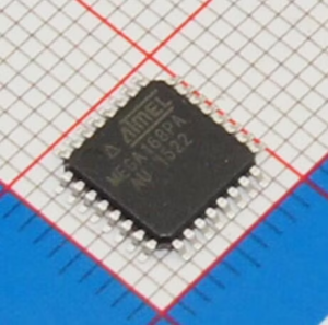
recuperar o programa IC ATmega168PA geralmente requer experiência em quebrar ou decodificar seu firmware criptografado para acessar o conteúdo bloqueado armazenado dentro deste microcontrolador ATmega168PA protegido. O ATMEGA168PA, um microcomputador ATmega168PA protetor, é projetado para proteger sua memória EEPROM, firmware e dados binários, garantindo que seu programa e código-fonte permaneçam protegidos contra acesso não autorizado. A engenharia reversa desempenha um papel fundamental no desbloqueio de seus mecanismos de proteção, permitindo que profissionais analisem e extraiam o software incorporado.
The I-bit is automatically set when a Return from Interrupt instruction – RETI – is executed. There are basically two types of interrupts. The first type is triggered by an event that sets the Interrupt Flag. For these interrupts, the Program Counter is vectored to the actual Interrupt Vector in order to execute the interrupt handling routine, and hardware clears the corresponding Interrupt Flag by Crack MCU Flash.
Interrupt Flags can also be cleared by writing a logic one to the flag bit position(s) to be cleared. If an interrupt condition occurs while the corresponding interrupt enable bit is cleared, the Interrupt Flag will be set and remembered until the interrupt is enabled, or the flag is cleared by software.
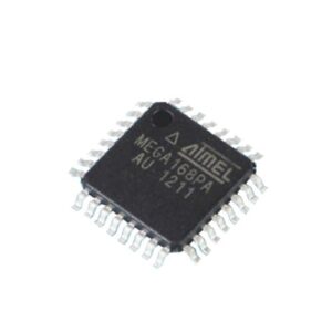
attack atmega168pa microcontroller protection and readout heximal file from atmega168pa flash memory and eeprom memory
Similarly, if one or more interrupt conditions occur while the Global Interrupt Enable bit is cleared, the corresponding Interrupt Flag(s) will be set and remembered until the Global Interrupt Enable bit is set, and will then be executed by order of priority.
The second type of interrupts will trigger as long as the interrupt condition is present. These interrupts do not necessarily have Interrupt Flags. If the interrupt condition disappears before the interrupt is enabled, the interrupt will not be triggered.
When the AVR exits from an interrupt, it will always return to the main program and execute one more instruction before any pending interrupt is served. Note that the Status Register is not automatically stored when entering an interrupt routine, nor restored when returning from an interrupt routine to replicate atmega168p avr mcu flash memory content file. This must be handled by software. When using the CLI instruction to disable interrupts, the interrupts will be immediately disabled. No interrupt will be executed after the CLI instruction, even if it occurs simultaneously with the CLI instruction. The following example shows how this can be used to avoid interrupts during the timed EEPROM write sequence.
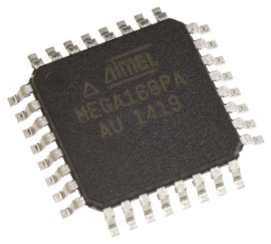
غالبًا ما يتطلب استرداد برنامج IC ATmega168PA خبرة في كسر أو فك تشفير البرامج الثابتة المشفرة للوصول إلى المحتوى المقفل المخزن داخل متحكم ATmega168PA الآمن هذا. تم تصميم ATMEGA168PA، وهو كمبيوتر ATmega168PA وقائي، لحماية ذاكرة EEPROM والبرامج الثابتة والبيانات الثنائية، مما يضمن حماية برنامجه ورمزه المصدر من الوصول غير المصرح به. تلعب الهندسة العكسية دورًا محوريًا في فتح آليات الحماية الخاصة به، مما يسمح للمحترفين بتحليل واستخراج البرامج المضمنة.
