Archive for the ‘Recover Chip’ Category
 Recover PIC18F4450 MCU Memory Data
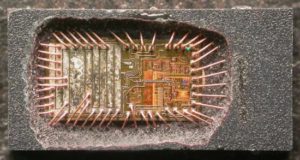
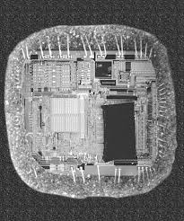
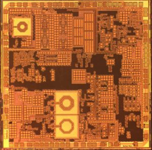
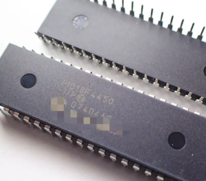
Recover PIC18F4450 MCU memory data starts from break microchip PIC18F4450 secured microcontroller tamper resistance system, readout flash memory program binary file and eeprom memory data heximal source code from unlocked PIC18F4450 encrypted microprocessor;
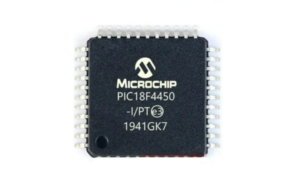
recover PIC18F4450 MCU memory data starts from break microchip PIC18F4450 secured microcontroller tamper resistance system, readout flash memory program binary file and eeprom memory data heximal source code from unlocked PIC18F4450 encrypted microprocessor;
The PC addresses bytes in the program memory. To prevent the PC from becoming misaligned with word instructions, the Least Significant bit of PCL is fixed to a value of ‘0’. The PC increments by 2 to address sequential instructions in the program memory of Recover PIC18F4450 MCU Memory Data.
The CALL, RCALL, GOTO and program branch instructions write to the program counter directly. For these instructions, the contents of PCLATH and PCLATU are not transferred to the program counter to Break IC S3F9454B Firmware.
recuperați datele de memorie PIC18F4450 MCU pornesc de la rupere microcip PIC18F4450 securizat microcontroler sistem de rezistență la manipulare, citirea fișierului binar al programului de memorie flash și codul sursă heximal de date de memorie eeprom de la microprocesorul criptat PIC18F4450 deblocat;
The Return Address Stack allows any combination of up to 31 program calls and interrupts to occur. The PC is pushed onto the stack when a CALL or RCALL instruction is executed or an interrupt is Acknowledged when Crack MCU Flash. The PC value is pulled off the stack on a RETURN, RETLW or a RETFIE instruction. PCLATU and PCLATH are not affected by any of the RETURN or CALL instructions.
The stack operates as a 31-word by 21-bit RAM and a 5-bit Stack Pointer, STKPTR. The stack space is not part of either program or data space. The Stack Pointer is readable and writable and the address on the top of the stack is readable and writable through the Top-of- Stack Special Function Registers to Recover Chip PIC16F913 Binary. Data can also be pushed to, or popped from the stack, using these registers from Recover PIC18F4450 MCU Memory Data.
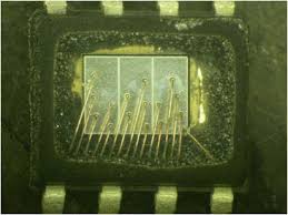
obnova dat paměti MCU PIC18F4450 začíná po rozbití mikročipu PIC18F4450 zabezpečený systém odolnosti proti neoprávněné manipulaci mikrokontroléru, načtení binárního souboru programu flash paměti a dat eeprom paměti heximální zdrojový kód z odemčeného šifrovaného mikroprocesoru PIC18F4450;
A CALL type instruction causes a push onto the stack. The Stack Pointer is first incremented and the location pointed to by the Stack Pointer is written with the contents of the PC (already pointing to the instruction following the CALL). A RETURN type instruction causes a pop from the stack to better support the process of Copy Chip AT89S8252 Flash
. The contents of the location pointed to by the STKPTR are transferred to the PC and then the Stack Pointer is decremented.
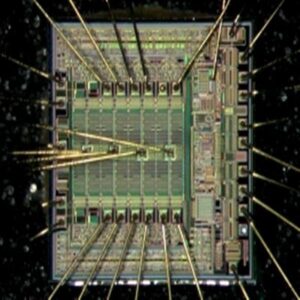
oporavak PIC18F4450 MCU memorijskih podataka počinje od prekida mikročipa PIC18F4450 osiguranog mikrokontrolera otpornog sustava protiv neovlaštenog otvaranja, očitavanja flash memorijskog programa binarne datoteke i eeprom memorijskih podataka heksimalni izvorni kod iz otključanog PIC18F4450 šifriranog mikroprocesora;
The Stack Pointer is initialized to ‘00000’ after all Resets. There is no RAM associated with the location corresponding to a Stack Pointer value of ‘00000’; this is only a Reset value. Status bits indicate if the stack is full or has overflowed or has underflowed by Copy Microcontroller PIC16F684 Firmware.
.
 Restore PIC18F4431 MCU Embedded Program
Restore PIC18F4431 MCU Embedded Program from internal memory including flash memory and eeprom memory needs to crack secured microcontroller PIC18F4431 fuse bit and extract binary source code or heximal data file from protective microprocessor PIC18F4431;
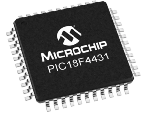
Restore PIC18F4431 MCU Embedded Program from internal memory including flash memory and eeprom memory needs to crack secured microcontroller PIC18F4431 fuse bit and extract binary source code or heximal data file from protective microprocessor PIC18F4431;
Only the top of the Return Address Stack (TOS) is readable and writable by Restore PIC18F4431 MCU Embedded Program. A set of three registers, TOSU:TOSH:TOSL, hold the contents of the stack location pointed to by the STKPTR register (see below Figure).
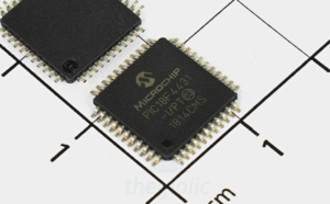
फ्लैश मेमोरी और ईप्रोम मेमोरी सहित आंतरिक मेमोरी से PIC18F4431 MCU एम्बेडेड प्रोग्राम को पुनर्स्थापित करने के लिए सुरक्षित माइक्रोकंट्रोलर PIC18F4431 फ्यूज बिट को क्रैक करने और सुरक्षात्मक माइक्रोप्रोसेसर PIC18F4431 से बाइनरी सोर्स कोड या हेक्सिमल डेटा फ़ाइल निकालने की आवश्यकता है;
This allows users to implement a software stack if necessary. After a CALL, RCALL or interrupt, the software can read the pushed value by reading the TOSU:TOSH:TOSL registers to facilitate the process of Copy IC PIC16F84A Binary. These values can be placed on a user defined software stack. At return time, the software can return these values to TOSU:TOSH:TOSL and do a return by Attack IC C8051F530 Firmware. The user must disable the global interrupt enable bits while accessing the stack to prevent inadvertent stack corruption.
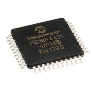
Restaurar o programa incorporado MCU PIC18F4431 da memória interna, incluindo memória flash e memória eeprom, precisa quebrar o bit de fusível do microcontrolador PIC18F4431 seguro e extrair o código-fonte binário ou arquivo de dados heximais do microprocessador de proteção PIC18F4431;
The STKPTR register (Register 5-1) contains the Stack Pointer value, the STKFUL (Stack Full) status bit and the STKUNF (Stack Underflow) status bits to Crack MCU. The value of the Stack Pointer can be 0 through 31. The Stack Pointer increments before values are pushed onto the stack and decrements after values are popped off the stack when Break Chip PIC16F917 Heximal.
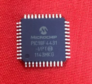
для восстановления встроенной программы MCU PIC18F4431 из внутренней памяти, включая флэш-память и память EEPROM, необходимо взломать защищенный предохранительный бит микроконтроллера PIC18F4431 и извлечь двоичный исходный код или шестнадцатеричный файл данных из защитного микропроцессора PIC18F4431;
On Reset, the Stack Pointer value will be zero. The user may read and write the Stack Pointer value. This feature can be used by a Real-Time Operating System (RTOS) for return stack maintenance by Copy Chip PIC16F870 Program. After the PC is pushed onto the stack 31 times (without popping any values off the stack), the STKFUL bit is set. The STKFUL bit is cleared by software or by a POR.
 Recover Microchip PIC18F4410 MCU Source Code
Recover Microchip PIC18F4410 MCU source code from flash program memory and eeprom data memory can help us extract protective PIC18F4410 microprocessor embedded firmware content from its flash after disable the security fuse, copy binary file or heximal data of source code after crack locked PIC18F4410 microcontroller;
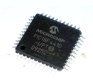
recuperar o código-fonte Microchip PIC18F4410 MCU da memória do programa flash e da memória de dados eeprom pode nos ajudar a extrair o conteúdo protetor do firmware incorporado do microprocessador PIC18F4410 de seu flash após desativar o fusível de segurança, copiar arquivo binário ou dados heximais do código-fonte após o microcontrolador PIC18F4410 bloqueado por crack;
Placing the BOR under software control gives the user the additional flexibility of tailoring the application to its environment without having to reprogram the device to change BOR configuration after the process of Recover Microchip PIC18F4410 MCU Source Code has been completed.
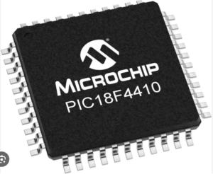
odzyskanie kodu źródłowego MCU Microchip PIC18F4410 z pamięci programu flash i pamięci danych eeprom może pomóc nam wyodrębnić zawartość wbudowanego oprogramowania sprzętowego mikroprocesora PIC18F4410 z jego pamięci flash po wyłączeniu bezpiecznika zabezpieczającego, skopiowaniu pliku binarnego lub danych szesnastkowych kodu źródłowego po złamaniu zablokowanego mikrokontrolera PIC18F4410;
It also allows the user to tailor device power consumption in software by eliminating the incremental current that the BOR consumes to support Break Chip Atmel Atmega48PV Heximal. While the BOR current is typically very small, it may have some impact in low-power applications.
Even when BOR is under software control, the BOR Reset voltage level is still set by the BORV1:BORV0 Configuration bits. It cannot be changed in software.
When BOR is enabled, the BOR bit always resets to ‘0’ on any BOR or POR event. This makes it difficult to determine if a BOR event has occurred just by reading the state of BOR alone to Break Microcontroller Samsung S3F9454 Software. A more reliable method is to simultaneously check the state of both POR and BOR.
This assumes that the POR bit is reset to ‘1’ in software immediately after any POR event. If BOR is ‘0’ while POR is ‘1’, it can be reliably assumed that a BOR event has occurred.

récupérer le code source du MCU Microchip PIC18F4410 à partir de la mémoire du programme flash et de la mémoire de données eeprom peut nous aider à extraire le contenu du microprocesseur de protection intégré au microprocesseur PIC18F4410 de son flash après avoir désactivé le fusible de sécurité, copier le fichier binaire ou les données heximales du code source après avoir verrouillé le microcontrôleur PIC18F4410 ;
When BOREN1:BOREN0 = 10, the BOR remains under hardware control and operates as previously described. Whenever the device enters Sleep mode of Break Microcontroller TI MSP430F448 Firmware, however, the BOR is automatically disabled. When the device returns to any other operating mode, BOR is automatically re-enabled.
This mode allows for applications to recover from brown-out situations, while actively executing code, when the device requires BOR protection the most. At the same time, it saves additional power in Sleep mode by eliminating the small incremental BOR current by Crack MCU Memory.
 Recover PIC18F4320 MCU Locked Heximal
Recover PIC18F4320 MCU locked heximal source code or binary firmware needs to decrypt protective microcontroller PIC18F4320 fuse bit, duplicate original program and data file from locked PIC18F4320 microprocessor flash memory and eeprom memory;
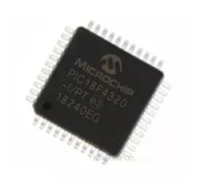
recover PIC18F4320 MCU locked heximal source code or binary firmware needs to decrypt protective microcontroller PIC18F4320 fuse bit, duplicate original program and data file from locked PIC18F4320 microprocessor flash memory and eeprom memory
PIC18F4320 devices implement a BOR circuit that provides the user with a number of configuration and power-saving options through Recover PIC18F4320 MCU Locked Heximal. The BOR is controlled by the BORV1:BORV0 and BOREN1:BOREN0 Configuration bits. There are a total of four BOR configurations which are summarized in below Table.
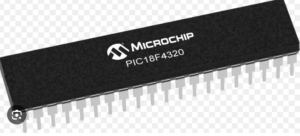
khôi phục mã nguồn heximal bị khóa PIC18F4320 MCU hoặc phần mềm nhị phân cần giải mã bit cầu chì PIC18F4320 của vi điều khiển bảo vệ, sao chép chương trình gốc và tệp dữ liệu từ bộ nhớ flash của bộ vi xử lý PIC18F4320 bị khóa và bộ nhớ eeprom
The BOR threshold is set by the BORV1:BORV0 bits. If BOR is enabled, any drop of VDD below VBOR (param- eter D005) for greater than TBOR (parameter 35) will reset the device. A Reset may or may not occur if VDD falls below VBOR for less than TBOR. The chip will remain in Brown-out Reset until VDD rises above VBOR.
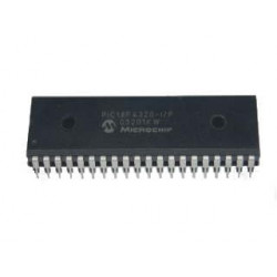
recuperar el código fuente heximal bloqueado de la MCU PIC18F4320 o el firmware binario necesita descifrar el bit fusible del microcontrolador protector PIC18F4320, duplicar el programa original y el archivo de datos de la memoria flash y la memoria eeprom del microprocesador PIC18F4320 bloqueado
If the Power-up Timer is enabled, it will be invoked after VDD rises above VBOR; it then will keep the chip in Reset for an additional time delay, TPWRT (parameter 33). If VDD drops below VBOR while the Power-up Timer is running, the chip will go back into a Brown-out Reset and the Power-up Timer will be initialized. Once VDD rises above VBOR, the Power-up Timer will execute the additional time delay.
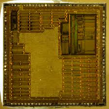
Recover PIC18F4320 MCU Locked Heximal
BOR and the Power-on Timer (PWRT) are independently configured. Enabling BOR Reset does not automatically enable the PWRT. When BOREN1:BOREN0 = 01, the BOR can be enabled or disabled by the user in software. This is done with the control bit, SBOREN (RCON<6>). Setting SBOREN enables the BOR to function as previously described. Clearing SBOREN disables the BOR entirely. The SBOREN bit operates only in this mode; otherwise it is read as ‘0’.
 Recover PIC18F4221 MCU Embedded Program
Recover PIC18F4221 MCU embedded program from locked PIC18F4221 microcontroller flash data memory and eeprom content memory, starts from break encrypted PIC18F4221 microprocessor protection by fuse bit and readout embedded firmware in the format of binary code or heximal file;
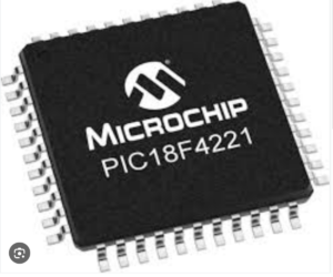
Recover PIC18F4221 MCU embedded program from locked PIC18F4221 microcontroller flash data memory and eeprom content memory, starts from break encrypted PIC18F4221 microprocessor protection by fuse bit and readout embedded firmware in the format of binary code or heximal file
This section discusses Resets generated by MCLR, POR and BOR and covers the operation of the various start-up timers from Recover PIC18F4221 MCU Embedded Program. Stack Reset events are covered in Section 5.1.2.4 “Stack Full and Underflow Resets”. WDT Resets are covered in Section 23.2 “Watchdog Timer (WDT)”.
The PIC18F4221 devices differentiate between various kinds of Reset:
a) Power-on Reset (POR)
b) MCLR Reset during normal operation
c) MCLR Reset during power-managed modes
d) Watchdog Timer (WDT) Reset (during execution)
e) Programmable Brown-out Reset (BOR)
f) RESET Instruction
g) Stack Full Reset
h) Stack Underflow Reset
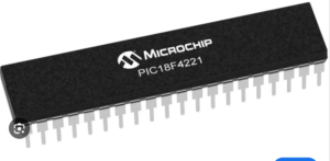
herstel PIC18F4221 MCU ingebed programma uit vergrendeld PIC18F4221 microcontroller flash datageheugen en eeprom inhoudsgeheugen, begint met het breken van gecodeerde PIC18F4221 microprocessorbescherming door zekeringsbit en uitlezen van ingebedde firmware in het formaat van binaire code of heximaal bestand;
A simplified block diagram of the on-chip Reset circuit is shown in below Figure.
Device Reset events are tracked through the RCON register (Register 4-1). The lower five bits of the regis- ter indicate that a specific Reset event has occurred. In most cases, these bits can only be cleared by the event and must be set by the application after the event of Crack MCU Memory.
The state of these flag bits, taken together, can be read to indicate the type of Reset that just occurred when Break MCU PIC16LF73 Heximal, This is described in more detail in Section 4.6 “Reset State of Registers”.
استعادة البرنامج المضمن PIC18F4221 MCU من ذاكرة بيانات فلاش المتحكم PIC18F4221 المقفلة وذاكرة محتوى eeprom، يبدأ من كسر حماية المعالجات الدقيقة المشفرة PIC18F4221 عن طريق بت المصهر والبرامج الثابتة المضمنة للقراءة بتنسيق الكود الثنائي أو الملف السداسي؛
The RCON register also has control bits for setting interrupt priority (IPEN) and software control of the BOR (SBOREN) in order to Decrypt LOCKED MCU PIC16LF72 Heximal. Interrupt priority is discussed in Section 9.0 “Interrupts”. BOR is covered in Section 4.4 “Brown-out Reset (BOR)”.
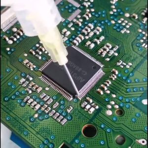
लॉक किए गए PIC18F4221 माइक्रोकंट्रोलर फ्लैश डेटा मेमोरी और ईप्रोम सामग्री मेमोरी से PIC18F4221 MCU एम्बेडेड प्रोग्राम को पुनर्प्राप्त करें, फ्यूज बिट द्वारा ब्रेक एन्क्रिप्टेड PIC18F4221 माइक्रोप्रोसेसर सुरक्षा से शुरू होता है और बाइनरी कोड या हेक्सिमल फ़ाइल के प्रारूप में एम्बेडेड फर्मवेयर को रीडआउट करता है;
 Recover PIC18F2682 Microcontroller Flash Program
Recover PIC18F2682 Microcontroller Flash Program and eeprom data program needs to decrypt protective MICROCHIP PIC18F2682 microprocessor tamper resistance system, copy original secured MCU PIC18F2682 embedded firmware to new chip;
recover PIC18F2682 microcontroller flash program and eeprom data program needs to decrypt protective MICROCHIP PIC18F2682 microprocessor tamper resistance system, copy original secured MCU PIC18F2682 embedded firmware to new chip;
In RC_IDLE mode, the CPU is disabled but the peripherals continue to be clocked from the internal oscillator block using the INTOSC multiplexer which is also critical for Recover PIC18F2682 Microcontroller Flash Program. This mode allows for controllable power conservation during Idle periods. From RC_RUN, this mode is entered by setting the IDLEN bit and executing a SLEEP instruction when Crack MCU Eeprom.

PIC18F2682 mikrodenetleyici flaş programını ve eeprom veri programını kurtarmak için koruyucu MICROCHIP PIC18F2682 mikroişlemci kurcalama direnci sistemini şifresini çözmek, orijinal güvenli MCU PIC18F2682 gömülü aygıt yazılımını yeni çipe kopyalamak gerekir;
If the device is in another Run mode, first set IDLEN, then set the SCS1 bit and execute SLEEP of Break chip ATMEGA861P code. Although its value is ignored, it is recommended that SCS0 also be cleared; this is to maintain software compatibility with future devices. The INTOSC multiplexer may be used to select a higher clock frequency by modifying the IRCF bits before executing the SLEEP instruction.
odzyskanie programu flash mikrokontrolera PIC18F2682 i danych eeprom; program wymaga odszyfrowania ochronnego systemu zabezpieczającego przed manipulacją mikroprocesora MICROCHIP PIC18F2682, skopiowanie oryginalnego zabezpieczonego oprogramowania wbudowanego MCU PIC18F2682 na nowy układ;
When the clock source is switched to the INTOSC multiplexer, the primary oscillator is shut down and the OSTS bit is cleared. If the IRCF bits are set to any non-zero value, or the INTSRC bit is set, the INTOSC output is enabled. The IOFS bit becomes set of Recover Microprocessor ATmega640V firmware, after the INTOSC output becomes stable, after an interval of TIOBST.
Clocks to the peripherals continue while the INTOSC source stabilizes. If the IRCF bits were previously at a non-zero value to Reverse Engineering MCU ATtiny48V eeprom or INTSRC was set before the SLEEP instruction was executed and the INTOSC source was already stable, the IOFS bit will remain set by Recover PIC18F2682 Microcontroller Flash Program. If the IRCF bits and INTSRC are all clear, the INTOSC output will not be enabled, the
IOFS bit will remain clear and there will be no indication of the current clock source. When a wake event occurs, the peripherals continue to be clocked from the INTOSC multiplexer. After a delay of TCSD following the wake event, the CPU begins executing code being clocked by the INTOSC multiplexer to support the process of Recover Microcontroller ATmega324V data, The IDLEN and SCS bits are not affected by the wakeup. The INTRC source will continue to run if either the WDT or the Fail-Safe Clock Monitor is enabled.
 Recover PIC18F2620 Microprocessor Eeprom Program
Microcontroller PIC16LF716 embedded firmware decryption is a process to unlock encrypted MICROCHIP MCU PIC16LF716 flash program memory and eeprom data memory, and retrieve embedded firmware from secured PIC16LF716 microprocessor by the binary file or heximal code;
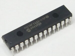
microcontroller PIC16LF716 embedded firmware decryption is a process to unlock encrypted MICROCHIP MCU PIC16LF716 flash program memory and eeprom data memory, and retrieve embedded firmware from secured PIC16LF716 microprocessor by the binary file or heximal code;
The Idle modes allow the controller’s CPU to be Recover PIC18F2620 Microprocessor Eeprom Program while the peripherals continue to operate. Selecting a particular Idle mode allows users to further manage power consumption.
If the IDLEN bit is set to a ‘1’ when a SLEEP instruction is executed, the peripherals will be clocked from the clock source selected using the SCS1:SCS0 bits; however, the CPU will not be clocked. The clock source status bits are not affected when Break IC ATmega640A Secured Flash. Setting IDLEN and executing a SLEEP instruction provides a quick method of switching from a given Run mode to its corresponding Idle mode.
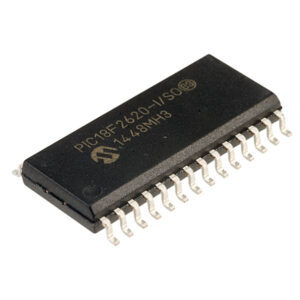
A descriptografia do firmware incorporado do microcontrolador PIC16LF716 é um processo para desbloquear a memória de programa flash criptografada do MICROCHIP MCU PIC16LF716 e a memória de dados eeprom, e recuperar o firmware incorporado do microprocessador PIC16LF716 protegido pelo arquivo binário ou código hexadecimal;
If the WDT is selected, the INTRC source will continue to operate. If the Timer1 oscillator is enabled, it will also continue to run. Since the CPU is not executing instructions, the only exits from any of the Idle modes are by interrupt, WDT time-out or a Reset to prevent the process of Decrypt Secured MCU ATMEGA128P Code.
When a wake event occurs, CPU execution is delayed by an interval of TCSD (parameter 38, Table 26-10) while it becomes ready to execute code when Crack MCU Flash. When the CPU begins executing code from Recover PIC18F2620 Microprocessor Eeprom Program, it resumes with the same clock source for the current Idle mode.
माइक्रोकंट्रोलर PIC16LF716 एम्बेडेड फर्मवेयर डिक्रिप्शन एन्क्रिप्टेड माइक्रोचिप MCU PIC16LF716 फ्लैश प्रोग्राम मेमोरी और ईप्रोम डेटा मेमोरी को अनलॉक करने और बाइनरी फ़ाइल या हेक्सिमल कोड द्वारा सुरक्षित PIC16LF716 माइक्रोप्रोसेसर से एम्बेडेड फर्मवेयर को पुनः प्राप्त करने की एक प्रक्रिया है;
For example, when waking from RC_IDLE mode, the internal oscillator block will clock the CPU and peripherals (in other words, RC_RUN mode). The IDLEN and SCS bits are not affected by the wake-up for the purpose of Reverse Engineering IC ATMEGA88PV Locked Flash. While in any Idle mode or the Sleep mode, a WDT time-out will result in a WDT wake-up to the Run mode currently specified by the SCS1:SCS0 bits.
 Microchip PIC18F2553 MCU Heximal Recovering
Microchip PIC18F2553 MCU heximal recovering can help engineer to restore embedded source code from secured microcontroller PIC18F2553 flash program memory and eeprom data memory, then engineer will be able to copy firmware binary file or heximal data to new microprocessor PIC18F2553;
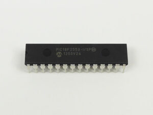
Microchip PIC18F2553 MCU heximal recovering can help engineer to restore embedded source code from secured microcontroller PIC18F2553 flash program memory and eeprom data memory, then engineer will be able to copy firmware binary file or heximal data to new microprocessor PIC18F2553;
The Timer1 oscillator should already be running prior to entering SEC_RUN mode which is necessary for Microchip PIC18F2553 MCU Heximal Recovering. If the T1OSCEN bit is not set when the SCS1:SCS0 bits are set to ‘01’, entry to SEC_RUN mode will not occur for Microchip PIC18F2520 Embedded Firmware Extraction. If the Timer1 oscillator is enabled, but not yet running, device clocks will be delayed until the oscillator has started. In such situa- tions, initial oscillator operation is far from stable and unpredictable operation may result.
การกู้คืนเลขฐานสิบหกของ MCU ของ Microchip PIC18F2553 ช่วยให้วิศวกรสามารถกู้คืนรหัสต้นฉบับที่ฝังไว้จากหน่วยความจำโปรแกรมแฟลชของไมโครคอนโทรลเลอร์ PIC18F2553 ที่ปลอดภัยและหน่วยความจำข้อมูล EEPROM จากนั้นวิศวกรก็จะสามารถคัดลอกไฟล์ไบนารีของเฟิร์มแวร์หรือข้อมูลเลขฐานสิบหกไปยังไมโครโปรเซสเซอร์ PIC18F2553 ใหม่ได้
On transitions from SEC_RUN to PRI_RUN mode, the peripherals and CPU continue to be clocked from the Timer1 oscillator while the primary clock is started. When the primary clock becomes ready, a clock switch back to the primary clock occurs (see below Figure). When the clock switch is complete, the T1RUN bit is cleared, the OSTS bit is set and the primary clock is providing the clock to Microchip MCU PIC16F870 Heximal Code Restoration. The IDLEN and SCS bits are not affected by the wake-up; the Timer1 oscillator continues to run.
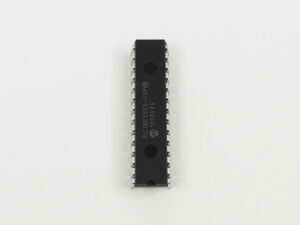
Восстановление шестнадцатеричных данных микроконтроллера Microchip PIC18F2553 может помочь инженеру восстановить встроенный исходный код из защищенной флэш-памяти программ микроконтроллера PIC18F2553 и памяти данных EEPROM, после чего инженер сможет скопировать двоичный файл прошивки или шестнадцатеричные данные на новый микропроцессор PIC18F2553;
In RC_RUN mode, the CPU and peripherals are clocked from the internal oscillator block using the INTOSC multiplexer. In this mode, the primary clock is shut down in order to Recover Freescale MCU MC9S12XDG128 Memory Program. When using the INTRC source, this mode provides the best power conservation of all the Run modes, while still executing code in the process of Microchip PIC18F2553 MCU Heximal Recovering. It works well for user applications which are not highly timing sensitive or do not require high-speed clocks at all times.
If the primary clock source is the internal oscillator block (either INTRC or INTOSC), there are no distinguishable differences between PRI_RUN and RC_RUN modes during MCU Crack execution. However, a clock switch delay will occur during entry to and exit from RC_RUN mode which can be carried out by Reverse Engineering Microchip PIC16F1913 Memory. Therefore, if the primary clock source is the internal oscillator block, the use of RC_RUN mode is not recommended.
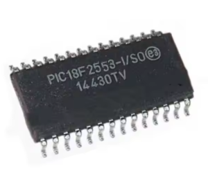
Phục hồi mã heximal MCU của Microchip PIC18F2553 có thể giúp kỹ sư khôi phục mã nguồn nhúng từ bộ nhớ chương trình flash và bộ nhớ dữ liệu eeprom của vi điều khiển được bảo mật PIC18F2553, sau đó kỹ sư sẽ có thể sao chép tệp nhị phân chương trình cơ sở hoặc dữ liệu heximal sang vi xử lý mới PIC18F2553;
 Recover PIC18F2539 Microcontroller Lost Heximal File
Recover PIC18F2539 microcontroller lost heximal file from original microchip MCU PIC18F2539 flash program memory and eeprom data memory, decrypt protective PIC18F2539 microprocessor’s security fuse bit and extract binary file or heximal source code from its embedded firmware;
Recover PIC18F2539 microcontroller lost heximal file from original microchip MCU PIC18F2539 flash program memory and eeprom data memory, decrypt protective PIC18F2539 microprocessor’s security fuse bit and extract binary file or heximal source code from its embedded firmware;
The length of the transition between clock sources is the sum of two cycles of the old clock source by Recover PIC18F2539 Microcontroller Lost Heximal File and three to four cycles of the new clock source. This formula assumes that the new clock source is stable.
Three bits indicate the current clock source and its status. They are:
- OSTS (OSCCON<3>)
- IOFS (OSCCON<2>)
- T1RUN (T1CON<6>)
In general, only one of these bits will be set while in a given power-managed mode. When the OSTS bit is set, the primary clock is providing the device clock by Break Nuvoton W78E054 MCU Flash. When the IOFS bit is set, the INTOSC output is providing a stable 8 MHz clock source to a divider that actually drives the device clock.
PIC18F2539 mikrodenetleyicisinin kaybolan heksimal dosyasını orijinal mikroçip MCU PIC18F2539 flaş program belleğinden ve eeprom veri belleğinden kurtarın, koruyucu PIC18F2539 mikroişlemcisinin güvenlik sigorta bitini şifresini çözün ve gömülü aygıt yazılımından ikili dosyayı veya heksimal kaynak kodunu çıkarın
When the T1RUN bit is set, the Timer1 oscillator is providing the clock. If none of these bits are set, then either the INTRC clock source is clocking the device, or the INTOSC source is not yet stable after Crack MCU Memory.
If the internal oscillator block is configured as the primary clock source by the FOSC3:FOSC0 Configuration bits in order to Attack Winbond W78E051A Protected Eeprom, then both the OSTS and IOFS bits may be set when in PRI_RUN or PRI_IDLE modes. This indicates that the primary clock (INTOSC output) is generating a stable 8 MHz output from Recover PIC18F2539 Microcontroller Lost Heximal File. Entering another power-managed RC mode at the same frequency would clear the OSTS bit.
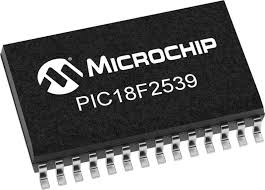
recuperați fișierul heximal pierdut al microcontrolerului PIC18F2539 din memoria programului flash original al microcipului MCU PIC18F2539 și memoria de date eeprom, decriptați bitul siguranței de securitate al microprocesorului PIC18F2539 și extrageți fișierul binar sau codul sursă heximal din firmware-ul său încorporat
Caution should be used when modifying a single IRCF bit through Reverse Engineering W78E52B Chip Data. If VDD is less than 3V, it is possible to select a higher clock speed than is supported by the low VDD. Improper device operation may result if the VDD/FOSC specifications are violated.
Executing a SLEEP instruction does not necessarily place the device into Sleep mode. It acts as the trigger to place the controller into either the Sleep mode or one of the Idle modes, depending on the setting of the IDLEN bit for the purpose of Winbond Microcontroller W78E0516 Embedded Binary Recovering.
récupérer le fichier hexadécimal perdu du microcontrôleur PIC18F2539 de la mémoire de programme flash PIC18F2539 et de la mémoire de données EEPROM d’origine du microprocesseur MCU PIC18F2539, décrypter le bit de fusible de sécurité du microprocesseur PIC18F2539 et extraire le fichier binaire ou le code source hexadécimal de son micrologiciel intégré
 Recover PIC18F2539 Microcontroller Embedded Eeprom
When PRI_IDLE mode is selected, the designated primary oscillator continues to run without interruption by Reverse Engineering Atmel MCU ATtiny48 Heximal. For all other power-managed modes, the oscillator using the OSC1 pin is disabled which will provide great benefit for Recover PIC18F2539 Microcontroller Embedded Eeprom. The OSC1 pin (and OSC2 pin, if used by the oscillator) will stop oscillating.
In Secondary Clock modes (SEC_RUN and SEC_IDLE), the Timer1 oscillator is operating and providing the device clock. The Timer1 oscillator may also run in all power-managed modes if required to clock Timer1 or Timer3.
In Internal Oscillator modes (RC_RUN and RC_IDLE), the internal oscillator block provides the device clock source through Decrypt Encrypted Microcontroller ATmega16PA Code.
The 31 kHz INTRC output can be used directly to provide the clock and may be enabled to support various special features regardless of the power-managed mode after MCU Crack Process (see Section 23.2 “Watchdog Timer (WDT)”, Section 23.3 “Two-Speed Start-up” and Section 23.4 “Fail-Safe Clock Monitor” for more information on WDT, Fail-Safe Clock Monitor and Two- Speed Start-up).
The INTOSC output at 8 MHz may be used directly to clock the device or may be divided down by the postscaler. The INTOSC output is disabled if the clock is provided directly from the INTRC output to Recover PIC18F2539 Microcontroller Embedded Eeprom.
If the Sleep mode is selected, all clock sources are stopped. Since all the transistor switching currents have been stopped for the purpose of Reverse Engineering Locked Chip ATmega164PA Firmware, Sleep mode achieves the lowest current consumption of the device (only leakage currents).
Enabling any on-chip feature that will operate during Sleep will increase the current consumed during Sleep. The INTRC is required to support WDT operation. The Timer1 oscillator may be operating to support a Real-Time Clock. Other features may be operating that do not require a device clock source after Attack Atmel Chip ATmega2561V Secure Code (i.e., MSSP slave, PSP, INTn pins and others). Peripherals that may add significant current consumption are listed in Section 26.2 “DC Characteristics: Power-Down and Supply Current”.
