Archive for the ‘Recover Chip’ Category
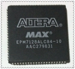
 Altera CPLD EPM7128ALC Embedded Eeprom Program Recovery
Altera CPLD EPM7128ALC Embedded Eeprom Program Recovery is a process to unlock security fuse bit of EPM7128 CPLD chip and extract eeprom firmware from CPLD’s secured memory in the format of JED;
Because MAX 7000A devices can be used in a mixed-voltage environment, they have been designed specifically to tolerate any possible power-up sequence. The VCCIO and VCCINT power planes can be powered in any order.
Signals can be driven into MAX 7000AE devices before and during power- up (and power-down) without damaging the device.
Additionally, MAX 7000AE devices do not drive out during power-up when breaking altera cpld epm7064aetc protection. Once operating conditions are reached, MAX 7000AE devices operate as specified by the user.
Altera CPLD EPM7128ALC recuperación del programa eeprom integrado es un proceso para desbloquear el bit de fusible de seguridad de EPM7128 chip CPLD y extraer el firmware eeprom de la memoria segura de CPLD en el formato de JED
MAX 7000AE device I/O pins will not source or sink more than 300 µA of DC current during power-up. All pins can be driven up to 5.75 V during hot-socketing, except the OE1 and GLCRn pins.
The OE1 and GLCRn pins can be driven up to 3.6 V during hot-socketing. After VCCINT and VCCIO reach the recommended operating conditions, these two pins are 5.0-V tolerant which can be used for recover embedded eeprom firmware of EPM7032VTC cpld chipset.
EPM7128A and EPM7256A devices do not support hot-socketing and may drive out during power-up.
 Recovering Altera CPLD EPM7032VTC44-15 Chipset Protection System
Recovering Altera CPLD EPM7032VTC44-15 Chipset Protection System is a process to crack altera cpld epm7032vtc44 security fuse bit and then copy embedded firmware out from its cpld flash memory;
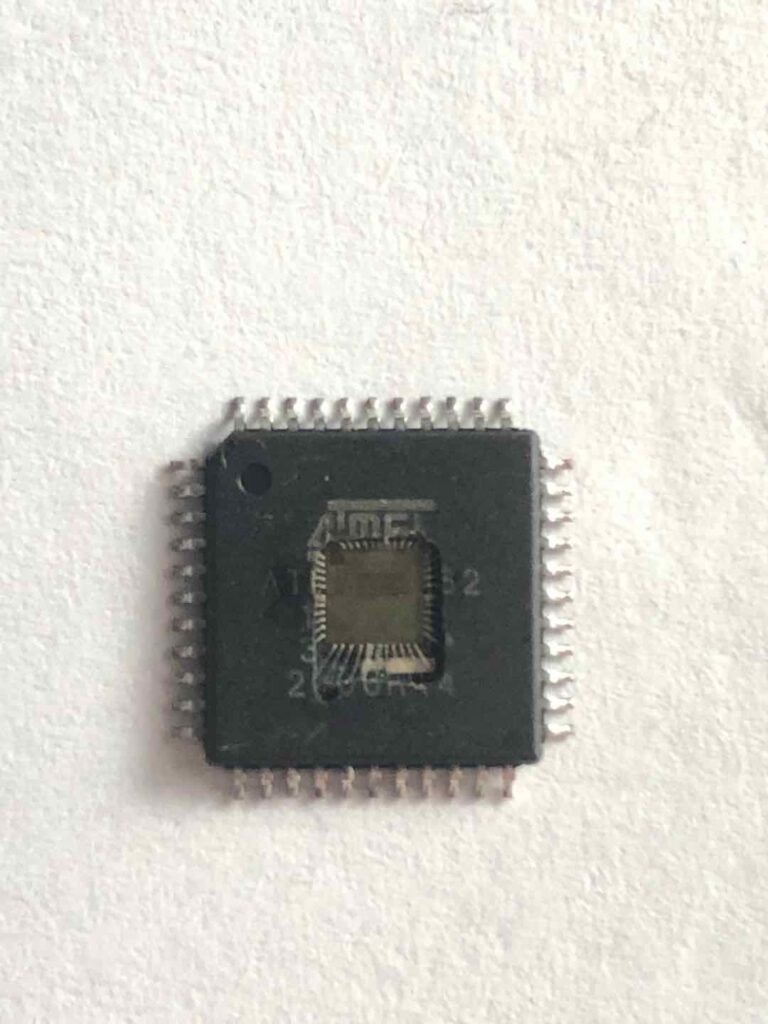
4.5-ns pin-to-pin logic delays with counter frequencies of up to 227.3 MHz
MultiVoltTM I/O interface enables device core to run at 3.3 V, while I/O pins are compatible with 5.0-V, 3.3-V, and 2.5-V logic levels;
Pin counts ranging from 44 to 256 in a variety of thin quad flat pack (TQFP), plastic quad flat pack (PQFP), ball-grid array (BGA), space- saving FineLine BGATM, and plastic J-lead chip carrier (PLCC) packages;
Supports hot-socketing in MAX 7000AE devices
Programmable interconnect array (PIA) continuous routing structure for fast, predictable performance
PCI-compatible
Bus-friendly architecture, including programmable slew-rate control
Open-drain output option
Programmable macrocell registers with individual clear, preset, clock, and clock enable controls
Programmable power-up states for macrocell registers in MAX 7000AE devices
Programmable power-saving mode for 50% or greater power reduction in each macrocell
Configurable expander product-term distribution, allowing up to 32 product terms per macrocell
Programmable security bit for protection of proprietary designs which can be used to attack cpld chip encrypted code
6 to 10 pin- or logic-driven output enable signals
Two global clock signals with optional inversion
Enhanced interconnect resources for improved routability
Fast input setup times provided by a dedicated path from I/O pin to macrocell registers
Programmable output slew-rate control
Programmable ground pins which can be used to copy lattice cpld program file
 Recover Texas Instrument MSP430G2252 MCU Flash Memory Firmware
Recover Texas Instrument MSP430G2252 MCU Flash Memory Firmware is a process to crack microprocessor msp430g2252 and extract locked source code from msp430g2252 flash memory;
Crystal Oscillator, XT1, Low-Frequency Mode
- To improve EMI on the XT1 oscillator, the following guidelines should be observed.
- Keep the trace between the device and the crystal as short as possible.
- Design a good ground plane around the oscillator pins.
- Prevent crosstalk from other clock or data lines into oscillator pins XIN and XOUT.
- Avoid running PCB traces underneath or adjacent to the XIN and XOUT pins.
- Use assembly materials and praxis to avoid any parasitic load on the oscillator XIN and XOUT pins.
- If conformal coating is used, ensure that it does not induce capacitive/resistive leakage between the oscillator pins.
- Do not route the XOUT line to the JTAG header to support the serial programming adapter as shown in other documentation. This signal is no longer required for the serial programming adapter when attack flash memory of microcontroller msp430g2312 .
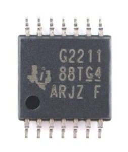
recuperare Texas Instrument MSP430G2252 firmware della memoria flash MCU è un processo per decifrare il microprocessore msp430g2252 ed estrarre il codice sorgente bloccato dalla memoria flash msp430g2252;
- Includes parasitic bond and package capacitance (approximately 2 pF per pin).
Because the PCB adds additional capacitance, it is recommended to verify the correct load by measuring the ACLK frequency. For a correct setup, the effective load capacitance should always match the specification of the used crystal.
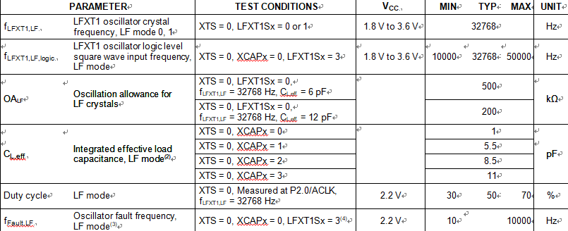
- Frequencies below the MIN specification set the fault flag. Frequencies above the MAX specification do not set the fault flag. Frequencies in between might set the flag.
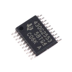
Wiederherstellen der Texas Instrument MSP430G2252 MCU-Flash-Speicher-Firmware ist ein Prozess zum Knacken des Mikroprozessors MSP430G2252 und Extrahieren des gesperrten Quellcodes aus dem Flash-Speicher MSP430G2252;
- Measured with logic-level input frequency but also applies to operation with crystals.
 Recover STMicro STM32F103C6 MCU Flash Full Content
Recover STMicro STM32F103C6 MCU Flash Full Content needs to unlock arm microcontroller stm32f103c6 memory and then copy extracted firmware to fresh MCU for cloning purpose;
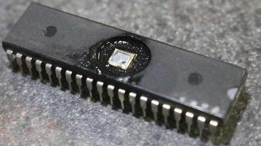
The current consumption is a function of several parameters and factors such as the operating voltage, ambient temperature, I/O pin loading, device software configuration, operating frequencies, I/O pin switching rate, program location in memory and executed binary code extracted.
The current consumption is measured as described in Figure 11: Current consumption measurement scheme.
All Run-mode current consumption measurements given in this section are performed with a reduced code that gives a consumption equivalent to Dhrystone 2.1 code for the purpose of restoring microcontroller stm32f103c4 flash source code.
The MCU is placed under the following conditions:
- l All I/O pins are in input mode with a static value at VDD or VSS (no load)
- l All peripherals are disabled except if it is explicitly mentioned
- l Prefetch in on (reminder: this bit must be set before clock setting and bus prescaling)
- l When the peripherals are enabled fPCLK1 = fHCLK, fPCLK2 = fHCLK
The parameters given in below Table are derived from tests performed under the ambient temperature and VDD supply voltage conditions summarized.
The Recovering MCU is placed under the following conditions:
- All I/O pins are in input mode with a static value at VDD or VSS (no load)
- All peripherals are disabled except if it is explicitly mentioned
- When the peripherals are enabled fPCLK1 = fHCLK, fPCLK2 = fHCLK, fADCCLK = fPCLK2/2
 ARM Microcontroller STM32F101C4 Locked Firmware Recovery
ARM Microcontroller STM32F101C4 Locked Firmware Recovery starts from cracking mcu stm32f101c4 flash memory and extract IC source code;

The STM32F101C4 value line embeds a nested vectored interrupt controller able to handle up to 41 maskable interrupt channels by Crack STM32F101C4 Microprocessor Flash Memory (not including the 16 interrupt lines of Cortex™-M3) and 16 priority levels.
Closely coupled NVIC gives low latency interrupt processing
Interrupt entry vector table address passed directly to the core
Closely coupled NVIC core interface
Allows early processing of interrupts
Processing of late arriving higher priority interrupts
Support for tail-chaining
Processor state automatically saved
Interrupt entry restored on interrupt exit with no instruction overhead
This hardware block provides flexible interrupt management features with minimal interrupt latency in the process of breaking arm mcu stm32f101rb flash memory.
Il ripristino del firmware bloccato STM32F101C4 del microcontrollore ARM inizia dal cracking della memoria flash MCU stm32f101c4 ed estrae il codice sorgente IC;
The external interrupt/event controller consists of 18 edge detector lines used to generate interrupt/event requests. Each line can be independently configured to select the trigger event (rising edge, falling edge, both) and can be masked independently.
Відновлення заблокованої мікропрограми мікроконтролера ARM STM32F101C4 починається зі злому флеш-пам’яті MCU STM32F101C4 і вилучення вихідного коду IC;
A pending register maintains the status of the interrupt requests. The EXTI can detect an external line with a pulse width shorter than the Internal APB2 clock period. Up to 80 GPIOs can be connected to the 16 external interrupt lines.
 Restore ARM Microprocessor STM32F100C8 Locked Program File
Restore ARM Microprocessor STM32F100C8 Locked Program File and rewrite the firmware into to new STM32F100C8 as cloning unit, firmware from MCU STM32F100C8’s flash memory can be readout directly;
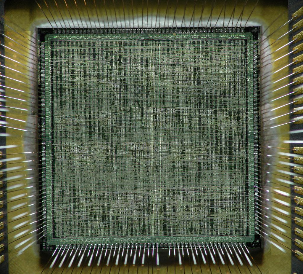
The ARM Cortex™-M3 processor is the latest generation of ARM processors for embedded systems. It has been developed to provide a low-cost platform that meets the needs of MCU implementation through reverse engineering stmicro arm mcu stm32f100c6 memory, with a reduced pin count and low-power consumption, while delivering outstanding computational performance and an advanced system response to interrupts.
The ARM Cortex™-M3 32-bit RISC processor features exceptional code-efficiency, delivering the high-performance expected from an ARM core in the memory size usually associated with 8- and 16-bit devices.
एआरएम माइक्रोप्रोसेसर STM32F100C8 लॉक किए गए प्रोग्राम फ़ाइल को पुनर्स्थापित करें और फर्मवेयर को क्लोनिंग यूनिट के रूप में नए STM32F100C8 में फिर से लिखें, एमसीयू STM32F100C8 की फ्लैश मेमोरी से फर्मवेयर को सीधे पढ़ा जा सकता है;
The STM32F100xx value line family having an embedded ARM core, is therefore compatible with all ARM tools and software.
Up to 128 Kbytes of embedded Flash memory is available for storing programs and data.
The CRC (cyclic redundancy check) calculation unit is used to get a CRC code from a 32-bit data word and a fixed generator polynomial.
استعادة المعالجات الدقيقة ARM STM32F100C8 ملف البرنامج المقفل وإعادة كتابة البرامج الثابتة إلى STM32F100C8 جديدة كوحدة استنساخ ، يمكن قراءة البرامج الثابتة من ذاكرة فلاش MCU STM32F100C8 مباشرة ؛
Among other applications, CRC-based techniques are used to verify data transmission or storage integrity. In the scope of the EN/IEC 60335-1 standard, they offer a means of verifying the Flash memory integrity. The CRC calculation unit helps compute a signature of the software during runtime, to be compared with a reference signature generated at link- time and stored at a given memory location.
Up to 8 Kbytes of embedded SRAM accessed (read/write) at CPU clock speed with 0 wait states.
 Duplicating DSP Microprocessor TMS320LF2407 Flash Program
Duplicating DSP Microprocessor TMS320LF2407 Flash Program to new MCU TMS320LF2407, the embedded firmware will be decrypted by MCU TMS320LF2407 flash and make new microcontroller copies;
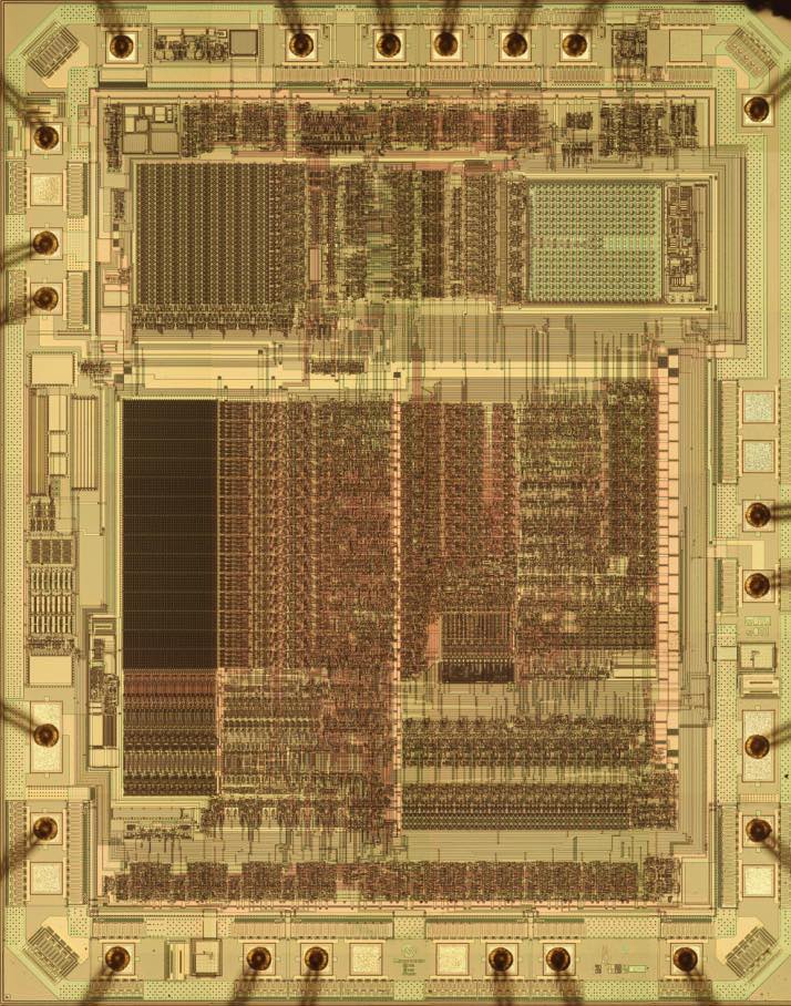
Output clock derived from SYSCLKOUT. XCLKOUT is either the same frequency, one-half the frequency, or one-fourth the frequency of SYSCLKOUT. This is controlled by bits 1:0 (XCLKOUTDIV) in the XCLK register.
At reset, XCLKOUT = SYSCLKOUT/4. The XCLKOUT signal can be turned off by setting XCLKOUTDIV to 3. The mux control for GPIO18 must also be set to XCLKOUT for this signal to propogate to the pin.
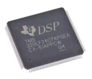
дублировать программу флэш-памяти микропроцессора TMS320LF2407 с защитой DSP на новый MCU TMS320LF2407, встроенная прошивка в двоичном или шестнадцатеричном виде будет расшифрована флэш-памятью MCU TMS320LF2407 и создаст новые копии микроконтроллера;
See GPIO19 and GPIO38. External oscillator input. Pin source for the clock is controlled by the XCLKINSEL bit in the XCLK register, GPIO38 is the default selection. This pin feeds a clock from an external 3.3-V oscillator. In this case, the X1 pin, if available, must be tied to GND and the on-chip crystal oscillator must be disabled through bit 14 in the CLKCTL register WHEN replicating dsp tms320lf2406 flash memory data.
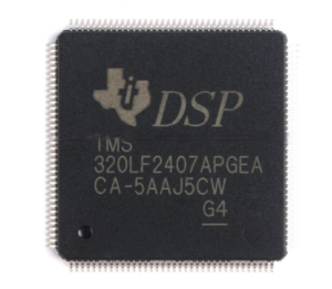
Duplizieren Sie das Flash-Speicherprogramm des DSP-geschützten Mikroprozessors TMS320LF2407 auf die neue MCU TMS320LF2407. Die eingebettete binäre oder hexadezimale Firmware wird vom MCU TMS320LF2407-Flash entschlüsselt und erstellt neue Kopien des Mikrocontrollers.
If a crystal or resonator is used, the XCLKIN path must be disabled by bit 13 in the CLKCTL register.NOTE: Designs that use the GPIO38/XCLKIN/TCK pin to supply an external clock for normal device operation may need to incorporate some hooks to disable this path during debug using the JTAG connector. This is to prevent contention with the TCK signal, which is active during JTAG debug sessions. The zero-pin internal oscillators may be used during this time to clock the device.
 Recover DSP Microcontroller TMS320F2811PB Flash Binary
Recover DSP Microcontroller TMS320F2811PB Flash Binary from its memory after crack mcu security fuse bit and extract the locked code from microprocessor;
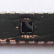
All output signals from the 28x devices (including XCLKOUT) are derived from an internal clock such that all output transitions for a given half-cycle occur with a minimum of skewing relative to each other.
The signal combinations shown in the following timing diagrams may not necessarily represent actual cycles. For actual cycle examples, see the appropriate cycle description section of this document.
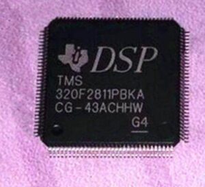
recuperați microcontrolerul DSP blocat TMS320F2811PB flash binar din memoria sa după bitul siguranței de securitate MCU protejat la crack TMS320F2811PB și extrageți codul sursă blocat, cum ar fi binar sau heximal, de la microprocesorul TMS320F2811PB, copiați firmware-ul original pe noul MCU pentru o clonare perfectă a microcomputerului;
This test load circuit is used to measure all switching characteristics provided in this document.

Input requirements in this data sheet are tested with an input slew rate of < 4 Volts per nanosecond (4 V/ns) at the device pin.
The data sheet provides timing at the device pin. For output timing analysis, the tester pin electronics and its transmission line effects must be taken into account.
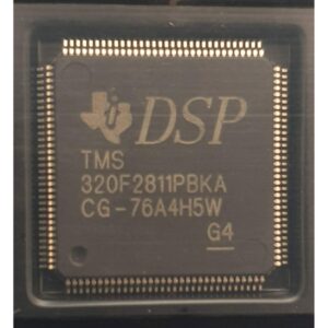
atkurkite užrakintą DSP mikrovaldiklio TMS320F2811PB „flash“ dvejetainį failą iš atminties po įtrūkimų apsaugoto TMS320F2811PB MCU saugos saugiklio bito ir ištraukite užrakintą šaltinio kodą, pvz., dvejetainį arba šešioliktainį, iš mikroprocesoriaus TMS320F2811PB, nukopijuokite originalią programinę-aparatinę įrangą į naują MCU, kad būtų tobulas mikrokompiuteris;
A transmission line with a delay of 2 ns or longer can be used to produce the desired transmission line effect. The transmission line is intended as a load only when recover dsp mcu tms320f28032 flash memory file. It is not necessary to add or subtract the transmission line delay (2 ns or longer) from the datasheet timing.
 Recover Texas DSP Microcpu TMS320F280230 Locked Flash Firmware
Recover Texas DSP Microcpu TMS320F280230 Locked Flash Firmware needs to crack protected cpu tms320f280230 memory and readout the embedded firmware from microcontroller;
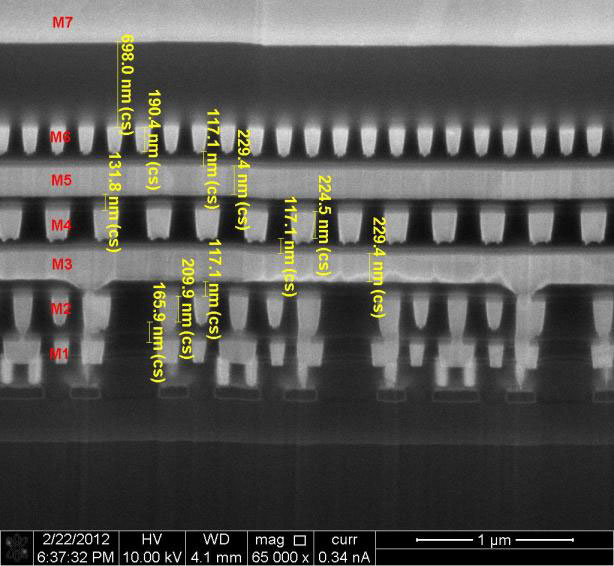
All output signals from the 28x devices (including XCLKOUT) are derived from an internal clock such that all output transitions for a given half-cycle occur with a minimum of skewing relative to each other.
The signal combinations shown in the following timing diagrams may not necessarily represent actual cycles. For actual cycle examples, see the appropriate cycle description section of this document when reverse dsp cpu tms320f28050 flash memory;
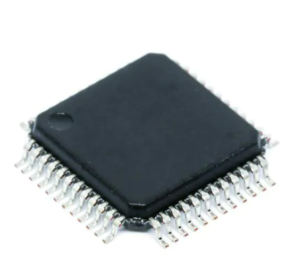
відновити TEXAS INSTRUMENT DSP, захищений мікроконтролер TMS320F280230PTT, заблоковану флеш-програму програмного забезпечення, яка потребує зламу захищеної пам’яті мікропроцесора TMS320F280230PTT і зчитування вихідного коду двійкового файлу або шістнадцяткових даних із зашифрованого MCU за допомогою пристрою READ-PROTECTION;
This test load circuit is used to measure all switching characteristics provided in this document.

A. Input requirements in this data sheet are tested with an input slew rate of < 4 Volts per nanosecond (4 V/ns) at the device pin.
B. The data sheet provides timing at the device pin. For output timing analysis, the tester pin electronics and its transmission line effects must be taken into account. A transmission line with a delay of 2 ns or longer can be used to produce the desired transmission line effect. The transmission line is intended as a load only.
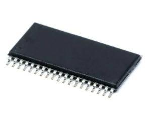
recuperar el microcontrolador seguro TEXAS INSTRUMENT DSP TMS320F280230PTT programa de firmware flash bloqueado necesita descifrar la memoria TMS320F280230PTT del microprocesador protegido y leer el código fuente del archivo binario o datos heximales de la MCU cifrada con un dispositivo de PROTECCIÓN DE LECTURA;
It is not necessary to add or subtract the transmission line delay (2 ns or longer) from the data sheet timing.
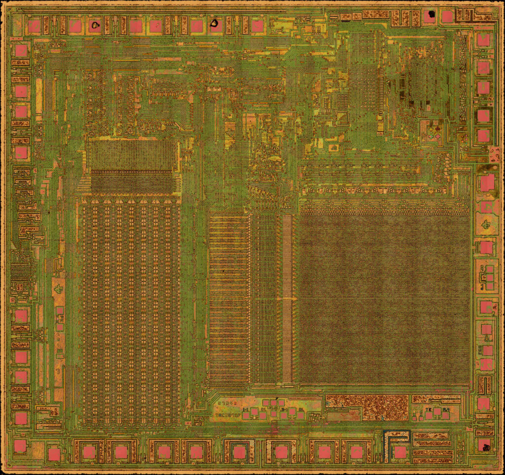
 TI DSP MCU TMS320F28015 Program Recovering
TI DSP MCU TMS320F28015 Program Recovering is a process to crack microcontroller tms320f28015 protection and readout MCU embedded firmware from flash memory;
The TMS320F28015 devices include the four-pin serial peripheral interface (SPI) module. The SPI is a high-speed synchronous serial-I/O port that allows a serial bit stream of programmed length in the process of attacking DSP Microcontroller TMS320F28232PGFA (one to eight bits) to be shifted into and out of the device at a programmable bit-transfer rate.
Normally, the SPI is used for communications between the DSP controller and external peripherals or another processor. Typical applications include external I/O or peripheral expansion through devices such as shift registers, display drivers, and ADCs. Multidevice communications are supported by the master/slave operation of the SPI.
The SPI module features include the following:
Four external pins:
- SPISOMI: SPI slave-output/master-input pin, or general-purpose bidirectional I/O pin
- SPISIMO: SPI slave-input/master-output pin, or general-purpose bidirectional I/O pin
- SPISTE: SPI slave-transmit-enable pin, or general-purpose bidirectional I/O pin
- SPICLK: SPI serial-clock pin, or general-purpose bidirectional I/O pin
Two operational modes: master and slave
Baud rate: 125 different programmable rates / 2.5 Mbps at 10-MHz SYSCLK
Data word format: one to eight data bits
Four clocking schemes controlled by clock polarity and clock-phase bits include:
Falling edge without phase delay: SPICLK active high. SPI transmits data on the falling edge of the SPICLK signal and receives data on the rising edge of the SPICLK in order to Crack Locked MCU TMS320F28069 Flash
Falling edge with phase delay: SPICLK active high. SPI transmits data one half-cycle ahead of the falling edge of the SPICLK signal and receives data on the falling edge of the SPICLK
Rising edge without phase delay: SPICLK inactive SPI transmits data on the rising edge of the SPICLK signal and receives data on the falling edge of the SPICLK signal to Reverse Engineering Microcontroller.
Rising edge with phase delay: SPICLK inactive SPI transmits data one half-cycle ahead of the falling edge of the SPICLK signal and receives data on the rising edge of the SPICLK signal.
Simultaneous receive and transmit operations to facilitate the progress (transmit function can be disabled in software)
Transmitter and receiver operations are accomplished through either interrupt-driven or polled algorithms.
Ten SPI module control registers: Located in control register frame beginning at address 7040h.
NOTE: All registers in this module are 8-bit registers that are connected to the 16-bit peripheral bus. When a register is accessed, the register data is in the lower byte (7 – 0), and the upper byte (15 – 8) is read as zeros. Writing to the upper byte has no effect.
