Archive for the ‘Recover Chip’ Category
 Recover MCU PIC16HV616 Eeprom
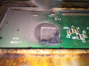
Recover MCU PIC16HV616 Eeprom content needs to crack microcomputer chip pic16hv616 and readout the embedded heximal from microcontroller pic16hv616 flash memory;
The data memory (see Figure 2-4) is partitioned into two banks, which contain the General Purpose Registers (GPR) and the Special Function Registers (SFR). The Special Function Registers are located in the first 32 locations of each bank.
PIC16F610/16HV610 Register locations 40h-7Fh in Bank 0 are General Purpose Registers, implemented as static RAM. PIC16F616/16HV616 Register locations 20h-7Fh in Bank 0 and A0h-BFh in Bank 1 are General Purpose Registers, implemented as static RAM. Register locations F0h-FFh in Bank 1 point to addresses 70h-7Fh in Bank 0. All other RAM is unimplemented and returns ‘0’ when read. The RP0 bit of the STATUS register is the bank select bit.
The register file is organized as 64 x 8 in the PIC16F610/16HV610 and 128 x 8 in the PIC16F616/16HV616. Each register is accessed, either directly or indirectly, through the File Select Register (FSR) (see Section 2.4 “Indirect Addressing, INDF and FSR Registers”) if copy pic16c72 Mcu software.
The Special Function Registers are registers used by the CPU and peripheral functions for controlling the desired operation of the device (see Table 2-1). These registers are static RAM. The special registers can be classified into two sets: core and peripheral. The Special Function Registers associated with the “core” are described in this section. Those related to the operation of the peripheral features are described in the section of that peripheral feature.
The STATUS register, shown in Register 2-1, contains:
· the arithmetic status of the ALU
· the Reset status
· the bank select bits for data memory (RAM)
The STATUS register can be the destination for any instruction, like any other register. If the STATUS register is the destination for an instruction that affects the Z, DC or C bits, then the write to these three bits is disabled. These bits are set or cleared according to the device logic. Furthermore, the TO and PD bits are not writable. Therefore, the result of an instruction with the STATUS register as destination may be different than intended.
For example, CLRF STATUS, will clear the upper three bits and set the Z bit. This leaves the STATUS register as ‘000u u1uu’ (where u = unchanged). The Program Counter (PC) is 13 bits wide. The low byte comes from the PCL register, which is a readable and writable register. The high byte (PC<12:8>) is not directly readable or writable and comes from PCLATH. On any Reset, the PC is cleared.
Figure 2-5 shows the two situations for the loading of the PC. The upper example in Figure 2-5 shows how the PC is loaded on a write to PCL (PCLATH<4:0> → PCH). The lower example in Figure 2-5 shows how the PC is loaded during aCALL or GOTO instruction (PCLATH<4:3> → PCH).
 Recover IC ATmega162PA Binary
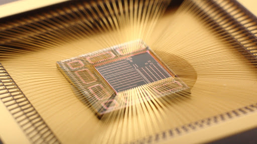
Recover IC ATmega162PA Binary from locked memory which include flash and eeprom, extract the code from mcu atmega162pa and copy heximal to new microcontroller atmega162pa;
The USART has to be initialized before any communication can take place. The initialization process normally consists of setting the baud rate, setting frame format and enabling the Transmitter or the Receiver depending on the usage.
For interrupt driven USART operation, the Global Interrupt Flag should be cleared (and interrupts globally disabled) when doing the initialization if Reverse mcu atmega461pv IC binary.
Before doing a re-initialization with changed baud rate or frame format, be sure that there are no ongoing transmissions during the period the registers are changed. The TXCn Flag can be used to check that the Transmitter has completed all transfers, an the RXC Flag can be used to check that there are no unread data in the receive buffer.
Note that the TXCn Flag must be cleared before each transmission (before UDRn is written) if it is used for this purpose. The following simple USART initialization binary examples show one assembly and one C function that are equal in functionality.
The examples assume asynchronous operation using polling (no interrupts enabled) and a fixed frame format. The baud rate is given as a function parameter. For the assembly binary, the baud rate parameter is assumed to be stored in the r17:r16 Registers after Reverse microcontroller atmega8p archive.
More advanced initialization routines can be made that include frame format as parameters, disable interrupts and so on. However, many applications use a fixed setting of the baud and control registers, and for these types of applications the initialization binary can be placed directly in the main routine, or be combined with initialization binary for other I/O modules.
The USART Transmitter is enabled by setting the Transmit Enable (TXEN) bit in the UCSRnB Register. When the Transmitter is enabled, the normal port operation of the TxDn pin is overridden by the USART and given the function as the Transmitter’s serial output.
The baud rate, mode of operation and frame format must be set up once before doing any transmissions. If synchronous operation is used, the clock on the XCKn pin will be overridden and used as transmission clock.
 Recover IC ATMEGA8V Firmware
We can Recover IC ATMEGA8V Firmware, please view the IC ATMEGA8V features for your reference:
On the IC ATMEGA8V devices, the DRT runs any time the device is powered up. The DRT operates on an internal oscillator. The processor is kept in Reset as long as the DRT is active when Recover IC firmware.
The DRT delay allows VDD to rise above VDD min. and for the oscillator to stabilize. The on-chip DRT keeps the devices in a Reset condition for approximately 18 ms after MCLR has reached a logic high (VIH MCLR) level if Recover IC firmware.
Programming GP3/MCLR/VPP as MCLR and using an external RC network connected to the MCLR input is not required in most cases. This allows savings in cost-sensitive and/or space restricted applications, as well as allowing the use of the GP3/MCLR/VPP pin as a general purpose input before Recover IC firmware.
The Device Reset Time delays will vary from chip-to- chip due to VDD, temperature and process variation. See AC parameters for details. Reset sources are POR, MCLR, WDT time-out and wake-up on pin change after Recover IC firmware.
See Section 9.9.2 “Wake-up from Sleep”, Notes 1, 2 and 3.
The WDT has a nominal time-out period of 18 ms, (with no prescaler). If a longer time-out period is desired, a prescaler with a division ratio of up to 1:128 can be assigned to the WDT (under software control) by writing to the OPTION register when Recover IC firmware.
Thus, a time-out period of a nominal 2.3 seconds can be realized. These periods vary with temperature, VDD and part-to-part process variations (see DC specs). Under worst-case conditions (VDD = Min., Temperature = Max., max. WDT prescaler), it may take several seconds before a WDT time-out occurs before Recover IC firmware.
9.6.2 WDT PROGRAMMING CONSIDERATIONS
The CLRWDT instruction clears the WDT and the postscaler, if assigned to the WDT, and prevents it from timing out and generating a device Reset after Recover IC firmware.
The SLEEP instruction resets the WDT and the postscaler, if assigned to the WDT. This gives the maximum Sleep time before a WDT wake-up Reset when Recover IC firmware.
 Recovery MCU PIC12CE673 Flash
Recovery MCU PIC12CE673 Flash memory protective content, the security fuse bit of microcontroller pic12ce673 will be cracked in order to readout the embedded heximal from mcu memory;
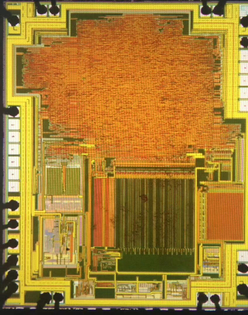
The PIC12C67X series fits perfectly in applications ranging from personal care appliances and security systems to low-power remote transmitters/receivers.
The EPROM technology makes customizing application programs (transmitter codes, appliance settings, receiver frequencies, etc.) extremely fast and convenient, while the EEPROM data memory (PIC12CE67X only) technology allows for the changing of calibration factors and security codes after breaking IC by brutel force.
The small footprint packages, for through hole or surface mounting, make this mcu series perfect for applications with space limitations. Low-cost, low-power, high performance, ease of use and I/O flexibility make the PIC12C67X series very versatile even in areas where no mcu use has been considered before (i.e., timer functions, replacement of “glue” logic and PLD’s in larger systems, coprocessor applications).
The PIC12C67X products are compatible with other members of the 14-bit PIC16CXXX families. The PIC12C67X devices are supported by a full featured macro assembler, a software simulator, an in-circuit emulator, a low-cost development programmer and a full-featured programmer.
A “C” compiler and fuzzy logic support tools are also available. A variety of frequency ranges and packaging options are available. Depending on application and production requirements, the proper device option can be selected using the information in the PIC12C67X Product Identification System section at the end of this data sheet when Recovery Mcu.
When placing orders, please use that page of the data sheet to specify the correct part number. For example, the PIC12C67X device “type” is indicated in the device number:
1. C, as in PIC12C671. These devices have EPROM type memory and operate over the standard voltage range.
2. LC, as in PIC12LC671. These devices have EPROM type memory and operate over an extended voltage range.
3. CE, as in PIC12CE674. These devices have EPROM type memory, EEPROM data memory and operate over the standard voltage range.
4. LCE, as in PIC12LCE674. These devices have EPROM type memory, EEPROM data memory and operate over an extended voltage range.
 Recover Microcontroller ATmega461PA Archive
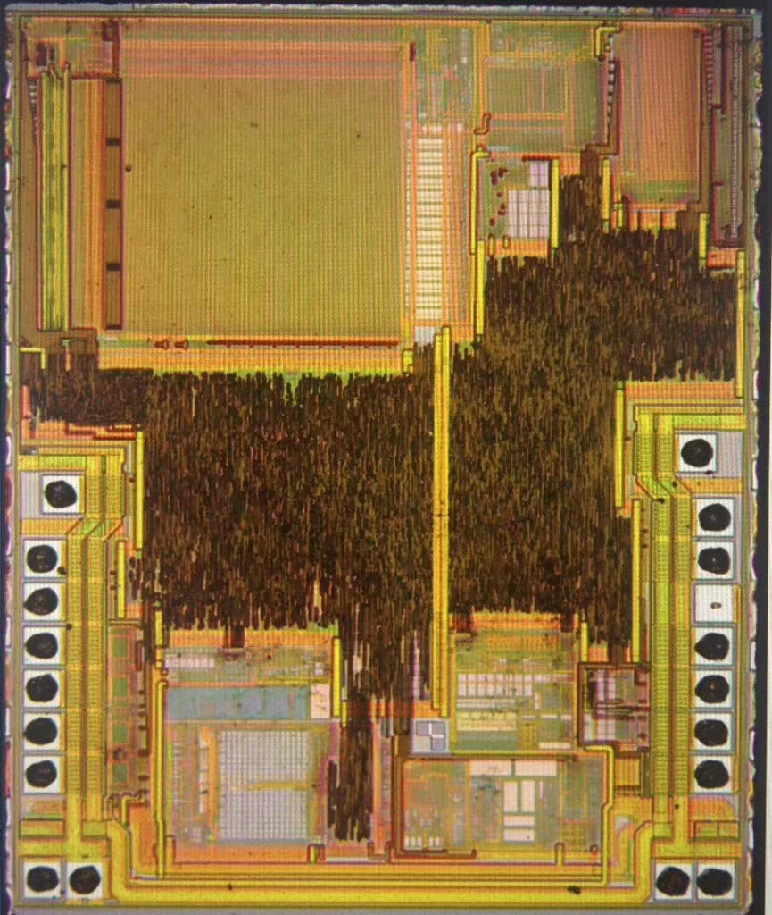
Recover Microcontroller ATmega461PA Archive from locked flash memory and readout the atmega461pa mcu program, rewrite it to new MCU atmega461pa for cloning;
When the SPI is enabled, the data direction of the MOSI, MISO, SCK, and SS pins is overridden according to Table 93. For more details on automatic port overrides.
The following code examples show how to initialize the SPI as a Master and how to perform a simple transmission. DDR_SPI in the examples must be replaced by the actual Data Direction Register controlling the SPI pins.
DD_MOSI, DD_MISO and DD_SCK must be replaced by the actual data direction bits for these pins. E.g. if MOSI is placed on pin PB5, replace DD_MOSI with DDB5 and DDR_SPI with DDRB. When the SPI is configured as a Slave, the Slave Select (SS) pin is always input. When SS is held low, the SPI is activated, and MISO becomes an output if configured so by the user after Reverse engineering attiny4313 Microcontroller code.
All other pins are inputs. When SS is driven high, all pins are inputs, and the SPI is passive, which means that it will not receive incoming data. Note that the SPI logic will be reset once the SS pin is driven high. The SS pin is useful for packet/byte synchronization to keep the slave bit counter synchronous with the master clock generator. When the SS pin is driven high, the SPI slave will immediately reset the send and receive logic, and drop any partially received data in the Shift Register.
When the SPI is configured as a Master (MSTR in SPCR is set), the user can determine the direction of the SS pin. If SS is configured as an output, the pin is a general output pin which does not affect the SPI system. Typically, the pin will be driving the SS pin of the SPI Slave.
If SS is configured as an input, it must be held high to ensure Master SPI operation. If the SS pin is driven low by peripheral circuitry when the SPI is configured as a Master with the SS pin defined as an input, the SPI system interprets this as another master selecting the SPI as a slave and starting to send data to it. To avoid bus contention, the SPI system takes the following actions if Recover attiny2313a Microcontroller heximal:
The MSTR bit in SPCR is cleared and the SPI system becomes a Slave. As a result of the SPI becoming a Slave, the MOSI and SCK pins become inputs. The SPIF Flag in SPSR is set, and if the SPI interrupt is enabled, and the I-bit in SREG is set, the interrupt routine will be executed.
Thus, when interrupt-driven SPI transmission is used in Master mode, and there exists a possibility that SS is driven low, the interrupt should always check that the MSTR bit is still set. If the MSTR bit has been cleared by a slave select, it must be set by the user to re-enable SPI Master mode.
 Recover Microcontroller ATmega261 Heximal
Recover Microcontroller ATmega261 Heximal from embedded flash memory, the mcu atmega261 will be unlocked by focus ion beam and locked code can be extracted from atmega261 memory;
If a write is performed to any of the five Timer/Counter2 Registers while its update busy flag is set, the updated value might get corrupted and cause an unintentional interrupt to occur.
The mechanisms for reading TCNT2, OCR2A, OCR2B, TCCR2A and TCCR2B are different. When reading TCNT2, the actual timer value is read. When reading OCR2A, OCR2B, TCCR2A and TCCR2B the value in the temporary storage register is read when breaking pic12f617 microcontroller.
When Timer/Counter2 operates asynchronously, some considerations must be taken. Warning: When switching between asynchronous and synchronous clocking of Timer/Counter2, the Timer Registers TCNT2, OCR2x, and TCCR2x might be corrupted.
A safe procedure for switching clock source is:
Disable the Timer/Counter2 interrupts by clearing OCIE2x and TOIE2.
Select clock source by setting AS2 as appropriate.
Write new values to TCNT2, OCR2x, and TCCR2x.
To switch to asynchronous operation: Wait for TCN2UB, OCR2xUB, and TCR2xUB.
Clear the Timer/Counter2 Interrupt Flags.
Enable interrupts, if needed.
The CPU main clock frequency must be more than four times the Oscillator frequency.
When writing to one of the registers TCNT2, OCR2x, or TCCR2x, the value is transferred to a temporary register, and latched after two positive edges on TOSC1.
The user should not write a new value before the contents of the temporary register have been transferred to its destination. Each of the five mentioned registers have their individual temporary register, which means that e.g. writing to TCNT2 does not disturb an OCR2x write in progress when Reverse engineering pic16hv610 microcontroller program.
To detect that a transfer to the destination register has taken place, the Asynchronous Status Register – ASSR has been implemented. When entering Power-save or ADC Noise Reduction mode after having written to TCNT2, OCR2x, or TCCR2x, the user must wait until the written register has been updated if Timer/Counter2 is used to wake up the device. Otherwise, the MICROCONTROLLER will enter sleep mode before the changes are effective.
This is particularly important if any of the Output Compare2 interrupt is used to wake up the device, since the Output Compare function is disabled during writing to OCR2x or TCNT2. If the write cycle is not finished, and the MICROCONTROLLER enters sleep mode before the corresponding OCR2xUB bit returns to zero, the device will never receive a compare match interrupt, and the MICROCONTROLLER will not wake up.
 Reverse Engineering IC ATmega261PV Code
Reverse Engineering IC ATmega261PV is a process to unlock mcu atmega261pv and extract out the embedded Code from microcontroller atmega261pv flash memory;
Combined with the WGM22 bit found in the TCCR2B Register, these bits control the counting sequence of the counter, the source for maximum (TOP) counter value, and what type of waveform generation to be used.
Modes of operation supported by the Timer/Counter unit are: Normal mode (counter), Clear Timer on Compare Match (CTC) mode, and two types of Pulse Width Modulation (PWM) modes (see “Modes of Operation” on page 178) if copy chip pic16c73a program.
The FOC2A bit is only active when the WGM bits specify a non-PWM mode. However, for ensuring compatibility with future devices, this bit must be set to zero when TCCR2B is written when operating in PWM mode.
When writing a logical one to the FOC2A bit, an immediate Compare Match is forced on the Waveform Generation unit. The OC2A output is changed according to its COM2A1:0 bits setting. Note that the FOC2A bit is implemented as a strobe. Therefore it is the value present in the COM2A1:0 bits that determines the effect of the forced compare after Recover mcu pic16f74a bin.
A FOC2A strobe will not generate any interrupt, nor will it clear the timer in CTC mode using OCR2A as TOP. The FOC2A bit is always read as zero. The FOC2B bit is only active when the WGM bits specify a non-PWM mode.
However, for ensuring compatibility with future devices, this bit must be set to zero when TCCR2B is written when operating in PWM mode. When writing a logical one to the FOC2B bit, an immediate Compare Match is forced on the Waveform Generation unit.
The OC2B output is changed according to its COM2B1:0 bits setting. Note that the FOC2B bit is implemented as a strobe. Therefore it is the value present in the COM2B1:0 bits that determines the effect of the forced compare before Recover chip pic16c71 code.
A FOC2B strobe will not generate any interrupt, nor will it clear the timer in CTC mode using OCR2B as TOP. The FOC2B bit is always read as zero.
If external pin modes are used for the Timer/Counter0, transitions on the T0 pin will clock the counter even if the pin is configured as an output. This feature allows software control of the counting.
The Timer/Counter Register gives direct access, both for read and write operations, to the Timer/Counter unit 8-bit counter. Writing to the TCNT2 Register blocks (removes) the Compare Match on the following timer clock. Modifying the counter (TCNT2) while the counter is running, introduces a risk of missing a Compare Match between TCNT2 and the OCR2x Registers.
The Output Compare Register A contains an 8-bit value that is continuously compared with the counter value (TCNT2). A match can be used to generate an Output Compare interrupt, or to generate a waveform output on the OC2A pin. The Output Compare Register B contains an 8-bit value that is continuously compared with the counter value (TCNT2). A match can be used to generate an Output Compare interrupt, or to generate a waveform output on the OC2B pin.
 Recover Chip PIC16C642 Binary
Recover Chip PIC16C642 Binary
We can Recover Chip PIC16C642 Binary, please view the Chip PIC16C642 features for your reference:
PIC16C64X & PIC16C66X devices are 28-pin and 40-pin EPROM-based members of the versatile PIC16CXXX family of low-cost, high-performance, CMOS, fully-static, 8-bit microcontrollers when Recover Chip. All PIC16/17 microcontrollers employ an advanced RISC architecture. The PIC16CXXX family has enhanced core features, eight-level deep stack, and multiple internal and external interrupt sources after Recover Chip.
The separate instruction and data buses of the Harvard architecture allow a 14-bit wide instruction word with the separate 8-bit wide data. The two-stage instruction pipeline allows all instructions to execute in a single-cycle, except for program branches (which require two cycles) if Recover Chip. A total of 35 instructions (reduced instruction set) are available. Additionally, a large register set gives some of the architectural innovations used to achieve a very high performance .
PIC16CXXX microcontrollers typically achieve a 2:1 code compression and a 4:1 speed improvement over other 8-bit microcontrollers in its class. The PIC16C641 has 128 bytes of RAM and the PIC16C642 has 176 bytes of RAM. Both devices have 22 I/O pins, and an 8-bit timer/counter with an 8-bit programmable prescaler when Recover Chip. In addition, they have two analog comparators with a programmable on-chip voltage reference module.
Program Memory has internal parity error detection circuitry with a Parity Error Reset. The comparator module is ideally suited for applications requiring a low-cost analog interface (e.g., battery chargers, threshold detectors, white goods controllers, etc.) before Recover Chip.
The PIC16C661 has 128 bytes of RAM and the PIC16C662 has 176 bytes of RAM. Both devices have 33 I/O pins, and an 8-bit timer/counter with an 8-bit programmable prescaler. They also have an 8-bit Parallel Slave Port. In addition, the devices have two analog comparators with a programmable on-chip voltage reference module when Recover Chip. Program Memory has internal parity error detection circuitry with a Parity Error Reset.
The comparator module is ideally suited for applications requiring a low-cost analog interface (e.g., battery chargers, threshold detectors, white goods controllers, etc.) if Recover Chip.
 Recover MCU ATMEGA861PA Program
We can Recover MCU ATMEGA861PA Program, please view the MCU ATMEGA861PA features for your reference:
For generating a waveform output in CTC mode, the OC2A output can be set to toggle its logical level on each compare match by setting the Compare Output mode bits to toggle mode (COM2A1:0 = 1). The OC2A value will not be visible on the port pin unless the data direction for the pin is set to output when Recover MCU program.
The waveform generated will have a maximum frequency of fOC2A = fclk_I/O/2 when OCR2A is set to zero (0x00). The waveform frequency is defined by the following equation: The N variable represents the prescale factor (1, 8, 32, 64, 128, 256, or 1024). As for the Normal mode of operation, the TOV2 Flag is set in the same timer clock cycle that the counter counts from MAX to 0x00. The fast Pulse Width Modulation or fast PWM mode (WGM22:0 = 3 or 7) provides a high frequency PWM waveform generation option. The fast PWM differs from the other PWM option by its single-slope operation after Recover MCU program.
The counter counts from BOTTOM to TOP then restarts from BOTTOM. TOP is defined as 0xFF when WGM22:0 = 3, and OCR2A when MGM22:0 = 7. In non-inverting Compare Output mode, the Output Compare (OC2x) is cleared on the compare match between TCNT2 and OCR2x, and set at BOTTOM when Recover MCU program.
In inverting Compare Output mode, the output is set on compare match and cleared at BOTTOM. Due to the single-slope operation, the operating frequency of the fast PWM mode can be twice as high as the phase correct PWM mode that uses dual-slope operation if Recover MCU program.
This high frequency makes the fast PWM mode well suited for power regulation, rectification, and DAC applications. High frequency allows physically small sized external components (coils, capacitors), and therefore reduces total system cost. In fast PWM mode, the counter is incremented until the counter value matches the TOP value. The counter is then cleared at the following timer clock cycle. The timing diagram for the fast PWM mode is shown in Figure 61. The TCNT2 value is in the timing diagram after Recover MCU.
shown as a histogram for illustrating the single-slope operation. The diagram includes non-inverted and inverted PWM outputs. The small horizontal line marks on the TCNT2 slopes represent compare matches between OCR2x and TCNT2. The Timer/Counter Overflow Flag (TOV2) is set each time the counter reaches TOP. If the interrupt is enabled, the interrupt handler routine can be used for updating the compare value if Recover MCU.
In fast PWM mode, the compare unit allows generation of PWM waveforms on the OC2x pin. Setting the COM2x1:0 bits to two will produce a non-inverted PWM and an inverted PWM output can be generated by setting the COM2x1:0 to three after Recover MCU program.
TOP is defined as 0xFF when WGM2:0 = 3, and OCR2A when WGM2:0 = 7 (See Table 86 on page 184). The actual OC2x value will only be visible on the port pin if the data direction for the port pin is set as output. The PWM waveform is generated by setting (or clearing) the OC2x Register at the compare match between OCR2x and TCNT2, and clearing (or setting) the OC2x Register at the timer clock cycle the counter is cleared (changes from TOP to BOTTOM) when Recover MCU program.
 Recover MCU PIC12C509 Program
Recover MCU PIC12C509 Program is a process to readout heximal file from embedded microcontroller pic12c509 after crack mcu fuse bit;
The high performance of the PIC12C5XX family can be attributed to a number of architectural features commonly found in RISC microprocessors. To begin with, the PIC12C5XX uses a Harvard architecture in which program and data are accessed on separate buses.
This improves bandwidth over traditional von Neumann architecture where program and data are fetched on the same bus. Separating program and data memory further allows instructions to be sized differently than the 8-bit wide data word. Instruction opcodes are 12-bits wide making it possible to have all single word instructions if break microcontroller pic16c716 hex.
A 12-bit wide program memory access bus fetches a 12-bit instruction in a single cycle. A two-stage pipeline overlaps fetch and execution of instructions. Consequently, all instructions (33) execute in a single cycle (1µs @ 4MHz) except for program branches.
The table below lists program memory (EPROM), data memory (RAM), ROM memory, and non-volatile (EEPROM) for each device. The PIC12C5XX device contains an 8-bit ALU and working register. The ALU is a general purpose arithmetic unit. It performs arithmetic and Boolean functions between data in the working register and any register file after attack pic16cr84 MCU memory
The ALU is 8-bits wide and capable of addition, subtraction, shift and logical operations. Unless otherwise mentioned, arithmetic operations are two’s complement in nature. In two-operand instructions, typically one operand is the W (working) register. The other operand is either a file register or an immediate constant. In single operand instructions, the operand is either the W register or a file register.
The register is an 8-bit working register used for ALU operations. It is not an addressable register. Depending on the instruction executed, the ALU may affect the values of the Carry (C), Digit Carry (DC), and Zero (Z) bits in the STATUS register.
Th e C and DC bits operate as a borrow and digit borrow out bit, respectively, in subtraction. See theSUBWF andADDWF instructions for examples. A simplified block diagram is shown in Figure 3-1, with the corresponding device pins described in Table 3-1. The PIC12C5XX can directly or indirectly address its register files and data memory.
All special function registers including the program counter are mapped in the data memory. The PIC12C5XX has a highly orthogonal (symmetrical) instruction set that makes it possible to carry out any operation on any register using any addressing mode. This symmetrical nature and lack of ‘special optimal situations’ make programming with the PIC12C5XX simple yet efficient. In addition, the learning curve is reduced significantly.