Archive for the ‘Recover Chip’ Category
 Decrypt Microprocessor ATmega1281 Eeprom
Decrypt Microprocessor ATmega1281 Eeprom and extract MCU ATmega1281 code from flash memory, prepare Microcontroller ATmega1281 unit clone by copy the firmware to new MCU unit;
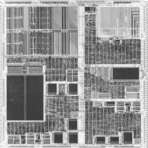
Decrypt Microprocessor ATmega1281 Eeprom and extract MCU ATmega1281 code from flash memory, prepare Microcontroller ATmega1281 unit clone by copy the firmware to new MCU unit
The Instruction Set for Serial Programming follows a 3-byte protocol and is shown in the following table: Stresses beyond those listed under “Absolute Maximum Ratings” may cause permanent damage to the device.
This is a stress rating only and functional operation of the device at these or any other conditions beyond those indicated in the operational sections of this specification is not implied if breaking PIC16F716 heximal memory.
Exposure to absolute maximum rating conditions for extended periods may affect device reliability. Under operating conditions, load capacitance for Port 0, ALE/PROG, and PSEN = 100 pF; load capacitance for all other outputs = 80 pF.
Typical values contained in this datasheet are based on simulations and characterization of other AVR microcontrollers manufactured on the same process technology. Min and Max values will be available after the device is characterized. The ATmega1281 is a low-power CMOS 8-bit microcontroller based on the AVR enhanced RISC architecture.
By executing powerful instructions in a single clock cycle, the ATmega1281 achieves throughputs approaching 1 MIPS per MHz allowing the system designer to optimize power consumption versus processing speed.
The AVR core combines a rich instruction set with 32 general purpose working registers. All the 32 registers are directly connected to the Arithmetic Logic Unit (ALU), allowing two independent registers to be accessed in one single instruction executed in one clock cycle.
The resulting architecture is more code efficient while achieving throughputs up to ten times faster than conventional CISC microcontrollers.
 Recover Microprocessor ATmega2561V Code
Recover Microprocessor ATmega2561V Code is a process to extract program and data from MCU ATmega2561V memory after crack microcontroller tamper resistance system;
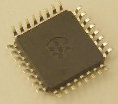
Port E is an 8-bit bi-directional I/O port with internal pull-up resistors (selected for each bit). The Port E output buffers have symmetrical drive characteristics with both high sink and source capability.
As inputs, Port E pins that are externally pulled low will source current if the pull-up resistors are activated when recover microprocessor code.
The Port E pins are tri-stated when a reset condition becomes active, even if the clock is not running. Port F serves as analog inputs to the A/D Converter. Port F also serves as an 8-bit bi-directional I/O port, if the A/D Converter is not used if attack microprocessor pic16c63a hex.
Port pins can provide internal pull-up resistors (selected for each bit). The Port F output buffers have symmetrical drive characteristics with both high sink and source capability. As inputs, Port F pins that are externally pulled low will source current if the pull-up resistors are activated.
The Port F pins are tri-stated when a reset condition becomes active, even if the clock is not running. If the JTAG interface is enabled, the pull-up resistors on pins PF7(TDI), PF5(TMS), and PF4(TCK) will be activated even if a reset occurs.
Port F also serves the functions of the JTAG interface. Port G is a 6-bit I/O port with internal pull-up resistors (selected for each bit). The Port G output buffers have symmetrical drive characteristics with both high sink and source capability when attack chip atmega8a binary.
As inputs, Port G pins that are externally pulled low will source current if the pull-up resistors are activated. The Port G pins are tri-stated when a reset condition becomes active, even if the clock is not running.
Port G also serves the functions of various special features of the ATmega2561 as listed on page 102.
Port H is a 8-bit bi-directional I/O port with internal pull-up resistors (selected for each bit). The Port H output buffers have symmetrical drive characteristics with both high sink and source capability. As inputs, Port H pins that are externally pulled low will source current if the pull-up resistors are activated. The Port H pins are tri-stated when a reset condition becomes active, even if the clock is not running before RECOVER MCU.
Port J is a 8-bit bi-directional I/O port with internal pull-up resistors (selected for each bit). The Port J output buffers have symmetrical drive characteristics with both high sink and source capability. As inputs, Port J pins that are externally pulled low will source current if the pull-up resistors are activated after recover microprocessor code.
The Port J pins are tri-stated when a reset condition becomes active, even if the clock is not running.
 Recover Microcontroller ATmega324V Data
Recover Microcontroller ATmega324V Data from program memory and data memory, unlock MCU ATmega324V security fuse by focus ion beam, then extract code from microprocessor ATmega324V;
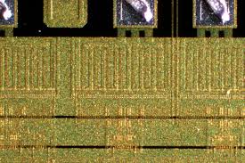
Pins XTAL1 and XTAL2 are input and output, respectively, of an inverting amplifier which can be configured for use as an On-Microcontroller Oscillator, as shown in Figure 22. Either a quartz crystal or a ceramic resonator may be used. This Crystal Oscillator is a full swing oscillator, with rail-to-rail swing on the XTAL2 output.
This is useful for driving other clock inputs and in noisy environments. The current consumption is higher than the “Low Power Crystal Oscillator”.
Note that the Full Swing Crystal Oscillator will only operate for Vcc = 2.7 – 5.5 volts. C1 and C2 should always be equal for both crystals and resonators. The optimal value of the capacitors depends on the crystal or resonator in use, the amount of stray capacitance, and the electromagnetic noise of the environment.
Some initial guidelines for choosing capacitors for use with crystals are given in Table 12. For ceramic resonators, the capacitor values given by the manufacturer should be used.
The frequency ranges are preliminary values. Actual values are TBD.
If 8 MHz frequency exceeds the specification of the device (depends on VCC), the CKDIV8 Fuse can be programmed in order to divide the internal frequency by 8. It must be ensured that the resulting divided clock meets the frequency specification of the device when chip pic16f870 program copying.
These options should only be used when not operating close to the maximum frequency of the device, and only if frequency stability at start-up is not important for the application. These options are not suitable for crystals.
These options are intended for use with ceramic resonators and will ensure frequency stability at start-up. They can also be used with crystals when not operating close to the maximum frequency of the device, and if frequency stability at start-up is not important for the application.
The frequency ranges are preliminary values. Actual values are TBD.
This option should not be used with crystals, only with ceramic resonators.
If 8 MHz frequency exceeds the specification of the device (depends on VCC), the CKDIV8 Fuse can be programmed in order to divide the internal frequency by 8. It must be ensured that the resulting divided clock meets the frequency specification of the device.
 Recover MCU ATmega324A Firmware
Recover MCU ATmega324A Firmware from embedded flash memory, unlock microcontroller ATmega324A needs to disable the security fuse bit and copy firmware out of processor;
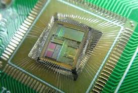
Note that this oscillator is used to time EEPROM and Flash write accesses, and these write times will be affected accordingly. If the EEPROM or Flash are written, do not calibrate to more than 8.8 MHz. Otherwise, the EEPROM or Flash write may fail.
The CAL7 bit determines the range of operation for the oscillator. Setting this bit to 0 gives the lowest frequency range, setting this bit to 1 gives the highest frequency range. The two frequency ranges are overlapping, in other words a setting of OSCCAL = 0x7F gives a higher frequency than OSCCAL = 0x80 if copy MCU atmega8l heximal.
The CAL6..0 bits are used to tune the frequency within the selected range. A setting of 0x00 gives the lowest frequency in that range, and a setting of 0x7F gives the highest frequency in the range. Incrementing CAL6..0 by 1 will give a frequency increment of less than 2% in the frequency range 7.3 – 8.1 MHz.
The 128 kHz internal Oscillator is a low power Oscillator providing a clock of 128 kHz. The frequency is nominal at 3V and 25°C. This clock may be select as the system clock by programming the CKSEL Fuses to “11” as shown in Table 16.
When this clock source is selected, start-up times are determined by the SUT Fuses as shown in Table 17. To drive the device from an external clock source, XTAL1 should be driven as shown in Figure 24. To run the device on an external clock, the CKSEL Fuses must be programmed to “0000” when Recover MCU stm32f107rct6 code.
When applying an external clock, it is required to avoid sudden changes in the applied clock frequency to ensure stable operation of the MCU. A variation in frequency of more than 2% from one clock cycle to the next can lead to unpredictable behavior. If changes of more than 2% is required, ensure that the MCU is kept in Reset during the changes.
Note that the System Clock Prescaler can be used to implement run-time changes of the internal clock frequency while still ensuring stable operation. Refer to “System Clock Prescaler” on page 48 for details. The device can output the system clock on the CLKO pin. To enable the output, the CKOUT Fuse has to be programmed.
This mode is suitable when the MCU clock is used to drive other circuits on the system. The clock also will be output during reset, and the normal operation of I/O pin will be overridden when the fuse is programmed. Any clock source, including the internal RC Oscillator, can be selected when the clock is output on CLKO. If the System Clock Prescaler is used, it is the divided system clock that is output.
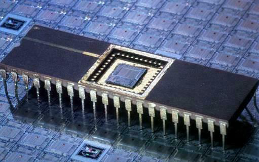
 Reverse Engineering ATMEL Chip AT32UC3C264C Flash
Reverse Engineering ATMEL Chip AT32UC3C264C Flash memory’s scheme diagram and cut off the security fuse bit by MCU cracking method, focus ion beam can be applied for Microcontroller code extraction;
One 4-Channel 20-bit Pulse Width Modulation Controller (PWM)
– Complementary outputs, with Dead Time Insertion
– Output Override and Fault Protection
Two Quadrature Decoders
One 16-channel 12-bit Pipelined Analog-To-Digital Converter (ADC)
– Dual Sample and Hold Capability Allowing 2 Synchronous Conversions
– Single-Ended and Differential Channels, Window Function
Two 12-bit Digital-To-Analog Converters (DAC), with Dual Output Sample System
Four Analog Comparators
Six 16-bit Timer/Counter (TC) Channels
– External Clock Inputs, PWM, Capture and Various Counting Capabilities
One Peripheral Event Controller
– Trigger Actions in Peripherals Depending on Events Generated from Peripherals or from Input Pins
– Deterministic Trigger after samsung microcontroller S3F9454 software breaking
– 34 Events and 22 Event Actions
Five Universal Synchronous/Asynchronous Receiver/Transmitters (USART)
– Independent Baudrate Generator, Support for SPI, LIN, IrDA and ISO7816 interfaces
– Support for Hardware Handshaking, RS485 Interfaces and Modem Line
Two Master/Slave Serial Peripheral Interfaces (SPI) with Chip Select Signals
One Inter-IC Sound (I2S) Controller
– Compliant with I2S Bus Specification
– Time Division Multiplexed mode
Three Master and Three Slave Two-Wire Interfaces (TWI), 400kbit/s I2C-compatible
QTouch® Library Support
– Capacitive Touch Buttons, Sliders, and Wheels
– QTouch® and QMatrix® Acquisition
On-Chip Non-intrusive Debug System
– Nexus Class 2+, Runtime Control, Non-Intrusive Data and flash Trace
– aWire™ single-pin flashming trace and debug interface muxed with reset pin
– NanoTrace™ provides trace capabilities through JTAG or aWire interface
3 package options
– 64-pin QFN/TQFP (45 GPIO pins) package
– 100-pin TQFP (81 GPIO pins)
– 144-pin LQFP (123 GPIO pins)
Two operating voltage ranges:
– Single 5V Power Supply
– Single 3.3V Power Supply
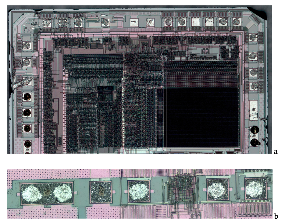
 Reverse Microchip MCU PIC16LF77 Flash
Reverse Microchip MCU PIC16LF77 Flash memory and readout hex of microcontroller PIC16LF77, status of processor PIC16LF77 can be opened and unlocking MCU’s tamper resistance system;
Low power, high speed CMOS FLASH technology
Fully static design
Wide operating voltage range: 2.0V to 5.5V
High Sink/Source Current: 25 mA
Industrial temperature range
Low power consumption:
– < 2 mA typical @ 5V, 4 MHz
– 20 µA typical @ 3V, 32 kHz
– < 1 µA typical standby current
PIC16F73/76 devices are available only in 28-pin packages, while PIC16F77 devices are available in 40-pin and 44-pin packages.
All devices in the PIC16F7X family share common architecture, with the following differences:
The PIC16F73 and PIC16F76 have one-half of the total on-chip memory of the PIC16LF77
The 28-pin devices have 3 I/O ports, while the 40/44-pin devices have 5
The 28-pin devices have 11 interrupts, while the 40/44-pin devices have 12
The 28-pin devices have 5 A/D input channels, while the 40/44-pin devices have 8
The Parallel Slave Port is implemented only on the 40/44-pin devices before Microchip mcu chip recovering
Additional information may be found in the PICmicro™ Mid-Range Reference Manual (DS33023), which may be obtained from your local Microchip Sales Representative or downloaded from the Microchip website.
The Reference Manual should be considered a complementary document to this data sheet, and is highly recommended reading for a better understanding of the device architecture and operation of the peripheral modules of Microchip mcu ST62T15C6 firmware attacking.
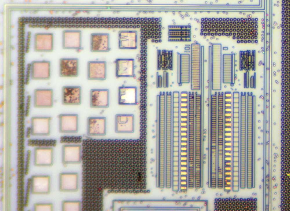
 Recovery Microcontroller PIC16LF76 Firmware
Recovery Microcontroller PIC16LF76 Firmware from flash memory and eeprom memory, crack MCU PIC16LF76 protective system and extract firmware from PIC16LF76 processor;
PIC16LF76 devices are available only in 28-pin packages, while PIC16LF76 devices are available in 40-pin and 44-pin packages. All devices in the PIC16F7X family share common architecture, with the following differences:
The PIC16LF76 have one-half of the total on-chip memory of the PIC16LF76
The 28-pin devices have 3 I/O ports, while the 40/44-pin devices have 5 if microcontroller samsung s3f9454 software breaking.
The 28-pin devices have 11 interrupts, while the 40/44-pin devices have 12
The 28-pin devices have 5 A/D input channels, while the 40/44-pin devices have 8.
The Parallel Slave Port is implemented only on the 40/44-pin devices
The available features are summarized in Table 1-1.
Block diagrams of the PIC16LF76 after Recovery.
Additional information may be found in the PICmicro™
Mid-Range Reference Manual (DS33023), which may be obtained from your local Microchip Sales Representative or downloaded from the Microchip website.
The Reference Manual should be considered a complementary document to this data sheet, and is highly recommended recoverying for a better understanding of the device architecture and operation of the peripheral modules Mcu pic16f688 software reading.
There are two memory blocks in each of these PICmicro® MICROCONTROLLERs. The Program Memory and Data Memory have separate buses so that concurrent access can occur and is detailed in this section.
The Program Memory can be recovery internally by user code (see Section 3.0). Additional information on device memory may be found in the PICmicro Mid-Range Reference Manual (DS33023).
 Reverse Microchip MCU PIC16F77 Flash
Reverse Microchip MCU PIC16F77 Flash memory and locate the fuse bit of microcontroller, and extract code from MCU PIC16F777;
- High performance RISC CPU
- Only 35 single word instructions to learn
- All single cycle instructions except for program branches which are two-cycle
- Operating speed: DC – 20 MHz clock input DC – 200 ns instruction cycle
- Up to 8K x 14 words of FLASH Program Memory, Up to 368 x 8 bytes of Data Memory (RAM)
- Pinout compatible to the PIC16C73B/74B/76/77
- Pinout compatible to the PIC16F873/874/876/877
- Interrupt capability (up to 12 sources)
- Eight level deep hardware stack
- Direct, Indirect and Relative Addressing modes
- Brown-out detection circuitry for
- Parallel Slave Port (PSP), 8-bits wide with
- Universal Synchronous Asynchronous Receiver
- 8-bit, up to 8-channel Analog-to-Digital converter
- Synchronous Serial Port (SSP) with SPI (Master
- Timer2: 8-bit timer/counter with 8-bit period
- Timer0: 8-bit timer/counter with 8-bit prescaler
- Timer1: 16-bit timer/counter with prescaler,
- Programmable code protection
- Power saving SLEEP mode
- Selectable oscillator options
- In-Circuit Serial Programming (ICSP) via two
- Watchdog Timer (WDT) with its own on-chip RCProcessor read access to program memory
- Power-on Reset (POR)
- Power-up Timer (PWRT) and
- Timer2: 8-bit timer/counter with 8-bit period
- Universal Synchronous Asynchronous Receiver
- Parallel Slave Port (PSP), 8-bits wide with
- Brown-out detection circuitry for
Oscillator Start-up Timer (OST) oscillator for reliable operation pins can be incremented during SLEEP via external crystal/clock register, prescaler and postscaler after breaking Microchip mcu pic12f509 eeprom.
- Two Capture, Compare, PWM modules
– Capture is 16-bit, max. resolution is 12.5 ns
– Compare is 16-bit, max. resolution is 200 ns
– PWM max. resolution is 10-bit mode) and I2C (Slave) Transmitter (USART/SCI) external RD, WR and CS controls (40/44-pin only) Brown-out Reset (BOR).
 Recovery Chip PIC18F2480 Eeprom
Recovery Chip PIC18F2480 Eeprom content and copy firmware to new microcontroller PIC18F2480 by reset the security fuse bit of MCU through MCU cracking technique;
This family of devices offers the advantages of all PIC18 chips – namely, high computational performance at an economical price – with the addition of high-endurance, Enhanced Flash eeprom memory.
In addition to these features, the PIC18F2480/2580/4480/4580 family introduces design enhancements that make these chips a logical choice for many high-performance, power-sensitive applications if Reverse mcu atmega461pv binary.
All of the devices in the PIC18F2480/2580/4480/4580 family incorporate a range of features that can significantly reduce power consumption during operation.
Key items include:
Alternate Run Modes: By clocking the controller from the Timer1 source or the internal oscillator block, power consumption during code execution can be reduced by as much as 90% after break ic flash atmega461v flash.
Multiple Idle Modes: The controller can also run with its CPU core disabled but the peripherals still active. In these states, power consumption can be reduced even further, to as little as 4% of normal operation requirements.
On-the-Fly Mode Switching: The power-managed modes are invoked by user code during operation, allowing the user to incorporate power-saving ideas into their application’s software design.
Lower Consumption in Key Modules: The power requirements for both Timer1 and the Watchdog Timer have been reduced by up to 80%, with typical values of 1.1 and 2.1 ìA, respectively before Reverse ic atmega162p eeprom.
Extended Instruction Set: In addition to the standard 75 instructions of the PIC18 instruction set, PIC18F2480/2580/4480/4580 devices also provide an optional extension to the core CPU functionality. The added features include eight additional instructions that augment indirect and indexed addressing operations and the implementation of Indexed Literal Offset Addressing mode for many of the standard PIC18 instructions.
 Decrypt Locked MCU PIC16LF72 Heximal
Decrypt Locked MCU PIC16LF72 and readout microcontroller PIC16LF72 Heximal from program memory and eeprom memory, normally the protection of MCU will be unlocked;
The WDT has a nominal time-out period of 18 ms, (with no prescaler). If a longer time-out period is desired, a prescaler with a division ratio of up to 1:128 can be assigned to the WDT (under software control) by writing to the OPTION register.
Thus, a time-out period of a nominal 2.3 seconds can be realized. These periods vary with temperature, VDD and part-to- part process variations (see DC specs) if break IC ATmega1284 firmware.
Under worst case conditions (VDD = Min., Temperature = Max., max. WDT prescaler), it may take several seconds before a WDT time-out occurs.
The CLRWDT instruction clears the WDT and the postscaler, if assigned to the WDT, and prevents it from timing out and generating a device RESET.
The SLEEP instruction resets the WDT and the postscaler, if assigned to the WDT. This gives the maximum SLEEP time before a WDT wake-up reset when reverse engineering mcu atmega1284pv firmware.
The TO, PD, and GPWUF bits in the STATUS register can be tested to determine if a RESET condition has been caused by a power-up condition, a MCLR or Watchdog Timer (WDT) reset.
A brown-out is a condition where device power (VDD) dips below its minimum value, but not to zero, and then recovers. The device should be reset in the event of a brown-out.
To reset PIC12C5XX devices when a brown-out occurs, external brown-out protection circuits may be built, This circuit will activate reset when VDD goes below Vz + 0.7V (where Vz = Zener voltage).* Refer to Figure 8-7 and Table 11-1 for internal weak pull-up on MCLR. This brown-out protection circuit employs Microchip Technology’s MCP809 microcontroller supervisor. The MCP8XX and MCP1XX family of supervisors provide push-pull and open collector outputs with both high and low active reset pins. There are 7 different trip point selections to accomodate 5V and 3V systems.