Archive for the ‘Recover Chip’ Category
 Recover IC AT89C4051 Heximal
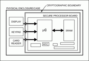
Recover IC AT89C4051 Heximal from flash memory and eeprom memory, decapsulate MCU AT89C4051 silicon package by MCU cracking, so the microprobe will be able to get access to the databus of Microcontroller AT89C4051
Recover IC AT89C4051 Heximal from flash memory and eeprom memory, decapsulate MCU AT89C4051 silicon package by MCU cracking, so the microprobe will be able to get access to the databus of Microcontroller AT89C4051;
Features
· Compatible with MCS®51 Products
· 4K Bytes of Reprogrammable Flash Memory
– Endurance: 1,000 Write/Erase Cycles
2.7V to 6V Operating Range
Fully Static Operation: 0 Hz to 24 MHz
Two-level Program Memory Lock
128 x 8-bit Internal RAM
15 Programmable I/O Lines
Two 16-bit Timer/Counters
Six Interrupt Sources
Programmable Serial UART Channel
Direct LED Drive Outputs
On-chip Analog Comparator
Low-power Idle and Power-down Modes
Brown-out Detection
Power-On Reset (POR)
Green (Pb/Halide-free/RoHS Compliant) Packaging
The AT89C4051 is a low-voltage, high-performance CMOS 8-bit microcontroller with
4K bytes of Flash programmable and erasable read-only memory. The device is manufactured using Atmel’s high-density nonvolatile memory technology and is compatible with the industry-standard MCS-51 instruction set. By combining a versatile 8-bit CPU with Flash on a monolithic chip, the Atmel AT89C4051 is a powerful microcontroller which provides a highly-flexible and cost-effective solution to many embedded control applications.
The AT89C4051 provides the following standard features: 4K bytes of Flash, 128 bytes of RAM, 15 I/O lines, two 16-bit timer/counters, a five-vector, two-level interrupt architecture, a full duplex serial port, a precision analog comparator, on-chip oscillator and clock circuitry. In addition, the AT89C4051 is designed with static logic for operation down to zero frequency and supports two software-selectable power saving modes. The Idle Mode stops the CPU while allowing the RAM, timer/counters, serial port and interrupt system to continue functioning. The power-down mode saves the RAM contents but freezes the oscillator disabling all other chip functions until the next hardware reset for MCU Attacking.
Circuit Engineering Company Limited continues to be recognized as the Southern China Leader in Services for IC Break, MCU attack, Chip Recover, Microcontroller Copy service. With the advancement of today’s modern circuit board technology, it is more important than ever to have specialists available to help you at a moment’s notice. Our engineering and commercial teams collectively have a vast amount of electronic experience covering field include Consumer Electronics, Industrial Automation Electronics, Wireless Communication Electronics., etc. For more information please contact us through email.
 Recover Microcontroller MC68HC908JB16 Firmware
Recover Microcontroller MC68HC908JB16 Firmware from flash memory include the program and data, the heximal file can be copied to new MCU MC68HC908JB16;
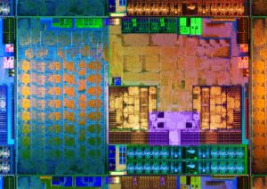
Recover Microcontroller MC68HC908JB16 Firmware from flash memory include the program and data, the heximal file can be copied to new MCU MC68HC908JB16
Features of the Microcontroller MC68HC908JB16 include the following:
High-performance M68HC08 architecture
Fully upward-compatible object code with M6805, M146805, and
M68HC05 families
Low-power design; fully static with stop and wait modes
6-MHz internal bus frequency
16,384 bytes of on-chip FLASH memory with security1 feature
384 bytes of on-chip random access memory (RAM)
Up to 21 general-purpose input/output (I/O) pins, including:
– 15 shared-function I/O pins
– 8-bit keyboard interrupt port
– 10mA high current drive for PS/2 connection on 2 pins (with USB module disabled)
– 1 dedicated I/O pin, with 25mA direct drive for infrared LED (32-pin package) if recover Microcontroller STM32F107RCT6 code
– 6 dedicated I/O pins, with 25mA direct drive for infrared LED on 2 pins and 10mA direct drive for normal LED on 4 pins (28-pin package)
Two 16-bit, 2-channel timer interface modules (TIM1 and TIM2) with selectable input capture, output compare, PWM capability on each channel, and external clock input option (TCLK)
Universal Serial Bus specification 2.0 low-speed functions:
– 1.5Mbps data rate
– On-chip 3.3V regulator
– Endpoint 0 with 8-byte transmit buffer and 8-byte receive buffer
– Endpoint 1 with 8-byte transmit buffer
– Endpoint 2 with 8-byte transmit buffer and 8-byte receive buffer
Serial communications interface module (SCI)
Dual clock generator modules (CGM) (32-pin package)
In-circuit programming capability using USB communication or standard serial link on PTA0 pin
System protection features:
– Optional computer operating properly (COP) reset
– Optional Low-voltage detection with reset
– Illegal opcode detection with reset
– Illegal address detection with reset
Master reset pin with internal pull-up and power-on reset
IRQ interrupt pin with internal pull-up and schmitt-trigger input
32-pin low-profile quad flat pack (LQFP) and 28-pin small outline
integrated circuit package (SOIC)
Features of the CPU08 include the following:
Enhanced HC05 programming model
Extensive loop control functions
16 addressing modes (eight more than the HC05)
16-bit index register and stack pointer
Memory-to-memory data transfers
Fast 8 × 8 multiply instruction
Fast 16/8 divide instruction
Binary-coded decimal (BCD) instructions
Optimization for controller applications
Third party C language support
 Recover Chip PIC16F913 Binary
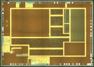
Recover Chip PIC16F913 Binary is a process of dumping heximal from MCU’s PIC16F913 flash memory, the status of Microcontroller PIC16F913 can be changed from locked to open by MCU Cracking technique
Recover Chip PIC16F913 Binary is a process of dumping heximal from MCU’s PIC16F913 flash memory, the status of Microcontroller PIC16F913 can be changed from locked to open by MCU Cracking technique;
High-Performance RISC CPU:
· Only 35 instructions to learn:
– All single-cycle instructions except branches
· Operating speed:
– DC – 20 MHz oscillator/clock input
– DC – 200 ns instruction cycle
· Program Memory Read (PMR) capability
· Interrupt capability
· 8-level deep hardware stack
· Direct, Indirect and Relative Addressing modes
Special Microcontroller Features:
· Precision Internal Oscillator:
– Factory calibrated to ±1%, typical
– Software selectable frequency range of
8 MHz to 125 kHz
– Software tunable
– Two-Speed Start-up mode
– External Oscillator fail detect for critical applications
– Clock mode switching during operation for power savings
· Software selectable 31 kHz internal oscillator
· Power-Saving Sleep mode
· Wide operating voltage range (2.0V-5.5V)
· Industrial and Extended temperature range
· Power-on Reset (POR)
· Power-up Timer (PWRT) and Oscillator Start-up
Timer (OST)
· Brown-out Reset (BOR) with software control option
· Enhanced Low-Current Watchdog Timer (WDT) with on-chip oscillator (software selectable nominal 268 seconds with full prescaler) with software enable
· Multiplexed Master Clear with pull-up/input pin
· Programmable code protection
· High-Endurance Flash/EEPROM cell:
– 100,000 write Flash endurance
– 1,000,000 write EEPROM endurance
– Flash/Data EEPROM retention: > 40 years
Low-Power Features:
· Standby Current:
– <100 nA @ 2.0V, typical
· Operating Current:
– 11 ìA @ 32 kHz, 2.0V, typical
– 220 ìA @ 4 MHz, 2.0V, typical
· Watchdog Timer Current:
– 1 ìA @ 2.0V, typical
Peripheral Features:
· Liquid Crystal Display module:
– Up to 60/96/168 pixel drive capability on 28/40/64-pin devices, respectively
– Four commons
· Up to 24/35/53 I/O pins and 1 input-only pin:
– High-current source/sink for direct LED drive
– Interrupt-on-change pin
– Individually programmable weak pull-ups
· In-Circuit Serial Programming™ (ICSP™) via two pins
· Analog comparator module with:
– Two analog comparators
– Programmable on-chip voltage reference (CVREF) module (% of VDD)
– Comparator inputs and outputs externally accessible
· A/D Converter:
– 10-bit resolution and up to 8 channels
· Timer0: 8-bit timer/counter with 8-bit
programmable prescaler
· Enhanced Timer1:
– 16-bit timer/counter with prescaler
– External Timer1 Gate (count enable)
– Option to use OSC1 and OSC2 as Timer1 oscillator if INTOSCIO or LP mode is selected
· Timer2: 8-bit timer/counter with 8-bit period register, prescaler and postscaler
· Addressable Universal Synchronous
Asynchronous Receiver Transmitter (AUSART)
· Up to 2 Capture, Compare, PWM modules:
– 16-bit Capture, max. resolution 12.5 ns
– 16-bit Compare, max. resolution 200 ns
– 10-bit PWM, max. frequency 20 kHz
· Synchronous Serial Port (SSP) with I2C™
 Recover IC STM32F107RCT6 Code
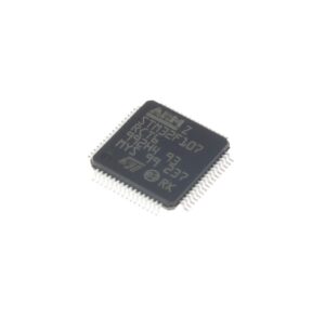
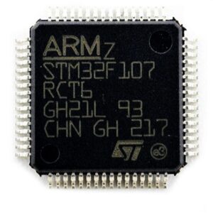
The STM32F107RCT6 is a high-performance ARM Cortex-M3 based microcontroller by STMicroelectronics, widely used in industrial, automotive, and embedded systems due to its integrated Ethernet MAC, USB OTG, CAN, and rich peripheral features. However, many applications implement protective measures to prevent firmware extraction, making it extremely difficult to readout, copy, or clone the original program. At [Your Company Name], we offer professional services to recover IC STM32F107RCT6 code, helping clients unlock, decrypt, and replicate protected firmware, even from locked or secured memory blocks.
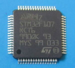
STM32F107RCT6 — это высокопроизводительный микроконтроллер на базе ARM Cortex-M3 от STMicroelectronics, широко используемый в промышленных, автомобильных и встраиваемых системах благодаря интегрированным Ethernet MAC, USB OTG, CAN и богатым периферийным функциям. Однако во многих приложениях реализованы защитные меры для предотвращения извлечения прошивки, что делает чрезвычайно сложным считывание, копирование или клонирование исходной программы. В Circuit Engineering Co.,LTD мы предлагаем профессиональные услуги по восстановлению кода IC STM32F107RCT6, помогая клиентам разблокировать, расшифровать и скопировать защищенную прошивку даже из заблокированных или защищенных блоков памяти.
Why Recover STM32F107RCT6 Firmware?
There are many valid reasons to recover embedded firmware from STM32 microcontrollers:
-
Legacy Support: Recovering firmware, binary, or heximal files from legacy systems where source code is lost.
-
System Migration: Transferring a protected program to a newer hardware platform.
-
Security Research: Analyzing secured firmware archives for vulnerabilities.
-
Product Cloning & Duplication: Replicating locked source code for batch production or testing.
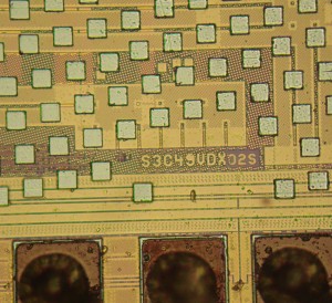
Recover IC STM32F107RCT6 code from MCU STM32F107RCT6 program memory, use MCU cracking technique to remove the security fuse by focus ion beam
Recover IC STM32F107RCT6 code from MCU STM32F107RCT6 program memory, use MCU cracking technique to remove the security fuse by focus ion beam;
Core: ARM 32-bit Cortex™-M3 CPU
– 72 MHz maximum frequency, 1.25 DMIPS/MHz (Dhrystone 2.1) performance at 0 wait state memory
LQFP100 14 × 14 mm
LQFP64 10 × 10 mm
LFBGA100 10 × 10 mm
– Single-cycle multiplication and hardware division
Memories
– 64 to 256 Kbytes of Flash memory
– 64 Kbytes of general-purpose SRAM Clock, reset and supply management
– 2.0 to 3.6 V application supply and I/Os
– POR, PDR, and programmable voltage detector (PVD)
– 3-to-25 MHz crystal oscillator
– Internal 8 MHz factory-trimmed RC
– Internal 40 kHz RC with calibration
– 32 kHz oscillator for RTC with calibration
STM32F107RCT6는 STMicroelectronics의 고성능 ARM Cortex-M3 기반 마이크로컨트롤러로, 이더넷 MAC, USB OTG, CAN 및 풍부한 주변 장치 기능을 통합하여 산업, 자동차 및 임베디드 시스템에서 널리 사용됩니다. 그러나 많은 애플리케이션에서 펌웨어 추출을 방지하기 위한 보호 기능이 구현되어 있어 원본 프로그램을 읽거나 복사하거나 복제하는 것이 매우 어렵습니다. Circuit Engineering Co.,LTD는 IC STM32F107RCT6 코드 복구 전문 서비스를 제공하여 고객이 잠기거나 보안된 메모리 블록에서도 보호된 펌웨어를 잠금 해제, 복호화 및 복제할 수 있도록 지원합니다.
Low power
– Sleep, Stop and Standby modes
– VBAT supply for RTC and backup registers 2 × 12-bit, 1 µs A/D converters (16 channels)
– Conversion range: 0 to 3.6 V
– Sample and hold capability
– Temperature sensor
– up to 2 MSPS in interleaved mode 2 × 12-bit D/A converters DMA: 12-channel DMA controller
– Supported peripherals: timers, ADCs, DAC, I2Ss, SPIs, I2Cs and USARTs
Up to 10 timers with pinout remap capability
– Up to four 16-bit timers, each with up to 4 IC/OC/PWM or pulse counter and quadrature (incremental) encoder input
– 1 × 16-bit motor control PWM timer with dead-time generation and emergency stop
– 2 × watchdog timers (Independent and Window)
– SysTick timer: a 24-bit downcounter
– 2 × 16-bit basic timers to drive the DAC Up to 14 communication interfaces with pinout remap capability
– Up to 2 × I2C interfaces (SMBus/PMBus)
STM32F107RCT6, entegre Ethernet MAC, USB OTG, CAN ve zengin çevre birimi özellikleri sayesinde endüstriyel, otomotiv ve gömülü sistemlerde yaygın olarak kullanılan STMicroelectronics tarafından üretilen yüksek performanslı bir ARM Cortex-M3 tabanlı mikrodenetleyicidir. Ancak birçok uygulama, ürün yazılımının çıkarılmasını önlemek için koruyucu önlemler uygular ve bu da orijinal programı okumayı, kopyalamayı veya klonlamayı son derece zorlaştırır. Circuit Engineering Co.,LTD’de, IC STM32F107RCT6 kodunu kurtarmak için profesyonel hizmetler sunuyoruz ve müşterilerin kilitli veya güvenli bellek bloklarından bile korumalı ürün yazılımını kilidini açmalarına, şifresini çözmelerine ve çoğaltmalarına yardımcı oluyoruz.
– Up to 5 USARTs (ISO 7816 interface, LIN, IrDA capability, modem control)
– Up to 3 SPIs (18 Mbit/s), 2 with a multiplexed I2S interface that offers audio class accuracy via advanced PLL schemes
– 2 × CAN interfaces (2.0B Active) with 512 bytes of dedicated SRAM
– USB 2.0 full-speed device/host/OTG controller with on-chip PHY that supports
HNP/SRP/ID with 1.25 Kbytes of dedicated SRAM
– 10/100 Ethernet MAC with dedicated DMA and SRAM (4 Kbytes): IEEE1588 hardware support, MII/RMII available on all packages
– Cortex-M3 Embedded Trace Macrocell™ Up to 80 fast I/O ports
– 51/80 I/Os, all mappable on 16 external interrupt vectors and almost all 5 V-tolerant CRC calculation unit, 96-bit unique ID
 Reverse Microchip PIC18F2220 MCU Flash Program
Reverse Microchip PIC18F2220 MCU Flash Program
During interrupts and subroutine calls, the return address PC is stored on the Stack. The Stack is effectively allocated in the general data SRAM, and consequently the Stack size is only limited by the total SRAM size and the usage of the SRAM from Reverse Microchip PIC18F2220 MCU Flash Program. After reset the Stack Pointer (SP) points to the highest address in the internal SRAM.
The SP is read/write accessible in the I/O memory space, enabling easy implementation of multiple stacks or stack areas. The data SRAM can easily be accessed through the five different addressing modes supported in the AVR CPU.The AVR architecture has two main memory spaces, the Program Memory and the Data Memory.
In addition, the XMEGA A3 features an EEPROM Memory for non-volatile data storage. All three memory spaces are linear and require no paging. The available memory size configurations are shown in ”Ordering Information” on page 2. In addition each device has a Flash memory signature row for calibration data, device identification, serial number etc. Non-volatile memory spaces can be locked for further write or read/write operations.
This prevents unrestricted access to the application software. The XMEGA A3 devices contains On-chip In-System Programmable Flash memory for program storage, see Figure 7-1 on page 10. Since all AVR instructions are 16- or 32-bits wide, each Flash address location is 16 bits. The Program Flash memory space is divided into Application and Boot sections.
Both sections have dedicated Lock Bits for setting restrictions on write or read/write operations. The Store Program Memory (SPM) instruction must reside in the Boot Section when used to write to the Flash memory before the code.
A third section inside the Application section is referred to as the Application Table section which has separate Lock bits for storage of write or read/write protection. The Application Table section can be used for storing non-volatile data or application software from MCU CRACK.
 Recover Freescale MCU MC9S12XDG128 Memory Program
Recover Freescale MCU MC9S12XDG128 Memory Program
The MC9S12XD family will retain the low cost, power consumption, EMC and code-size efficiency advantages currently enjoyed by users of Freescale’s existing 16-Bit MC9S12 MCU Family.
Based around an enhanced S12 core, the MC9S12XD family will deliver 2 to 5 times the performance of a 25-MHz S12 whilst retaining a high degree of pin and code compatibility with the S12 which makes the Recover Freescale MCU MC9S12XDG128 Memory Program becomes more value effectively.
The MC9S12XD family introduces the performance boosting XGATE module. Using enhanced DMA functionality, this parallel processing module offloads the CPU by providing high-speed data processing and transfer between peripheral modules, RAM, Flash EEPROM and I/O ports. Providing up to 80 MIPS of performance additional to the CPU, the XGATE can access all peripherals, Flash EEPROM and the RAM block.
The MC9S12XD family is composed of standard on-chip peripherals including up to 512 Kbytes of Flash EEPROM, 32 Kbytes of RAM, 4 Kbytes of EEPROM, six asynchronous serial communications interfaces (SCI), three serial peripheral interfaces (SPI), an 8-channel IC/OC enhanced capture timer, an 8-channel, 10-bit analog-to-digital converter, a 16-channel, 10-bit analog-to-digital converter, an 8-channel pulse-width modulator (PWM), five CAN 2.0 A, B software compatible modules (MSCAN12), two inter-IC bus blocks, and a periodic interrupt timer. The MC9S12XD family has full 16-bit data paths throughout.
The non-multiplexed expanded bus interface available on the 144-pin versions allows an easy interface to external memories The inclusion of a PLL circuit allows power consumption and performance to be adjusted to suit operational requirements from Recover Freescale MCU MC9S12XDG128 Memory Program. System power consumption can be further improved with the new “fast exit from stop mode” feature.
In addition to the I/O ports available in each module, up to 25 further I/O ports are available with interrupt capability allowing wake-up from stop or wait mode.
Family members in 144-pin LQFP will be available with external bus interface and parts in 112-pin LQFP or 80-pin QFP package without external bus interface. See Appendix E Derivative Differences for package options.
 Recover Microchip PIC18F2423 memory program
Recover Microchip PIC18F2423 Memory Program
Recover Microchip PIC18F2423 memory program includes recover the content from both eeprom and flash, so it is necessary to get a better knowledge of the internal structure:
12-bit,up to 13-channel Analog-to-Digital
Converter module (A/D):
– Auto-acquisition capability
– Conversion available during Sleep
Dualanalog comparators with input multiplexing
High-currentsink/source 25 mA/25 mA
Threeprogrammable external interrupts
Fourinput change interrupts of IC recoverion
Upto 2 Capture/Compare/PWM (CCP) modules, one with Auto-Shutdown (28-pin devices)
EnhancedCapture/Compare/PWM (ECCP) module (40/44-pin devices only):
– One, two or four PWM outputs
– Selectable polarity
– Programmable dead time
– Auto-shutdown and auto-restart
MasterSynchronous Serial Port (MSSP) module supporting 3-wire SPI (all 4 modes) and I2C™
Master and Slave modes
EnhancedUSART module:
– Supports RS-485, RS-232 and LIN 1.2
– RS-232 operation using internal oscillator block (no external crystal required)
– Auto-wake-up on Start bit
– Auto-Baud Detect
Run:CPU on, peripherals on
Idle:CPU off, peripherals on
Sleep:CPU off, peripherals off
Idlemode currents down to 5.8 ìA, typical
Sleepmode current down to 0.1 ìA, typical
Timer1Oscillator: 1.8 ìA, 32 kHz, 2V
WatchdogTimer: 2.1 ìA
FourCrystal modes, up to 25 MHz
4xPhase Lock Loop (available for crystal and Two-SpeedOscillator Start-up internal oscillators)
TwoExternal RC modes, up to 4 MHz
TwoExternal Clock modes, up to 25 MHz
Internaloscillator block:
– 8 user-selectable frequencies, from 31 kHz to 8 MHz
– Provides a complete range of clock speeds from 31 kHz to 32 MHz when used with PLL
– User-tunable to compensate for frequency drift
Secondaryoscillator using Timer1 @ 32 kHz
Fail-SafeClock Monitor:
– Allows for safe shutdown if external clock stops
 Recover Winbond W78ERD2 Chip Eeprom Data
Recover Winbond W78ERD2 Chip Eeprom Data
Clock and crystal oscillator are all playing the important roles in Recover Winbond W78ERD2 Chip Eeprom Data.
The W78ERD2 is designed to be used with either a crystal oscillator or an external clock. Internally, the clock is divided by two before it is used by default. This makes the W78ERD2 relatively insensitive to duty cycle variations in the clock.
Crystal Oscillator
The W78ERD2 incorporates a built-in crystal oscillator. To make the oscillator work, a crystal must be connected across pins XTAL1 and XTAL2. In addition, a load capacitor must be connected from each pin to ground, and a resistor must also be connected from XTAL1 to XTAL2 to provide a DC bias when the crystal frequency is above 24 MHz.
External Clock
An external clock should be connected to pin XTAL1. Pin XTAL2 should be left unconnected. The XTAL1 input is a CMOS-type input, as required by the crystal oscillator. As a result, the external clock signal should have an input one level of greater than 3.5 volts.
 Winbond MCU W78E365 Heximal Data Restoration
Winbond MCU W78E365 Heximal Data Restoration means the content from both the eeprom and flash can be extracted and read out by the programmer directly,
The W78E365 architecture consists of a core controller surrounded by various registers, four general purpose I/O ports, one special purpose programmable 4-bits I/O port, 512 bytes of RAM, three timer/counters, a serial port, and an internal 74373 latch and 74244 buffer which can be switched to port2.
The processor supports 111 different opcodes and references both a 64K program address space and a 64 K data storage space.
The internal data RAM in the W78E62B is 512 bytes. It is divided into two banks: 256 bytes of scratchpad RAM and 256 bytes of AUX-RAM. These RAMs are addressed by different ways.
RAM 0H-127H can be addressed directly and indirectly as the same as in 8051. Address pointers are R0 and R1 of the selected register RAM 128H-255H can only be addressed indirectly as the same as in 8051 when Winbond MCU W78E365 Heximal Data Restoration.
Address pointers are R0, R1 of the selected registers internal program memory, an access to AUX-RAM will not affect the Ports P0, P2, WR and RD.
AUX-RAM 0H-255H is addressed indirectly as the same way to access external data memory with the MOVX instruction. Address pointer are R0 and R1 of the selected register bank and DPTR register.
An access to external data memory locations higher than 255H will be performed with the MOVX instruction in the same way as in the 8051. The AUX-RAM is disable after a reset.
Setting the bit 4 in CHPCON register will enable the access to AUX-RAM. When AUX-RAM is enabled the instructions of “MOVX @Ri” will always access to on-chip AUX-RAM after Winbond MCU W78E365 Heximal Data Restoration.
 Nuvoton Microcomputer W78E51B Encrypted Heximal Recovery
If engineer has ever tried to execute Nuvoton Microcomputer W78E51B Encrypted Heximal Recovery, it is necessary to have a general idea about the Microcomputer W78E51B features:
• Fully static design 8-bit CMOS microcontroller
• Wide supply voltage of 4.5V to 5.5V
• 128 bytes of on-chip scratchpad RAM
• 4 KB On-chip Flash EPROM
• 64 KB program memory address space
• 64 KB data memory address space
• Four 8-bit bi-directional ports
• One extra 4-bit bit-addressable I/O port, additional INT2 / INT3
(available on 44-pin PLCC/QFP package)
• Two 16-bit timer/counters
• One full duplex serial port(UART)
• Watchdog Timer
• Seven sources, two-level interrupt capability
• EMI reduction mode
• Built-in power management
• Code protection mechanism
The W78E51B architecture consists of a core controller surrounded by various registers, five general purpose I/O ports, 128 bytes of RAM, two timer/counters, and a serial port. The processor supports 111 different opcodes and references both a 64K program address space and a 64K data storage space.
In order to be more suitable for I/O, an extra 4-bit bit-addressable port P4 and two external interrupt
INT2 , INT3 has been added to either the PLCC or QFP 44 pin package. And description follows:
INT2 / INT3
Two additional external interrupts, INT2 and INT3 , whose functions are similar to those of external interrupt 0 and 1 in the standard 80C52 after Nuvoton Microcomputer W78E51B Encrypted Heximal Recovery. The functions/status of these interrupts are determined/shown by the bits in the XICON (External Interrupt Control) register. The XICON register is bit-addressable but is not a standard register in the standard 80C52. Its address is at 0C0H. To set/clear bits in the XICON register, one can use the “SETB (/CLR) bit” instruction. For example, “SETB 0C2H” sets the EX2 bit of XICON.
PX3: External interrupt 3 priority high if set EX3: External interrupt 3 enable if set
IE3: If IT3 = 1, IE3 is set/cleared automatically by hardware when interrupt is detected/serviced IT3: External interrupt 3 is falling-edge/low-level triggered when this bit is set/cleared by software PX2: External interrupt 2 priority high if set
EX2: External interrupt 2 enable if set
IE2: If IT2 = 1, IE2 is set/cleared automatically by hardware when interrupt is detected/serviced IT2: External interrupt 2 is falling-edge/low-level triggered when this bit is set/cleared by software
