Archive for the ‘Recover Chip’ Category
 Recover Secured MCU STM32F405RG Binary Program
Recover secured MCU STM32F405RG binary program or heximal file from its locked flash memory needs to crack arm encrypted STM32F405RG microcontroller fuse bit and extract encrypted microprocessor STM32F405RG embedded firmware;
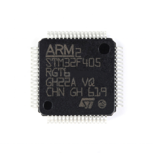
Recover secured MCU STM32F405RG binary program or heximal file from its locked flash memory needs to crack arm encrypted STM32F405RG microcontroller fuse bit and extract encrypted microprocessor STM32F405RG embedded firmware
In the realm of embedded systems, where efficiency, versatility, and performance are paramount, the STM32F405 microcontroller stands out as a formidable choice. Developed by STMicroelectronics, the STM32F405 series combines advanced features, ample connectivity options, and robust processing capabilities, making it a preferred solution for a diverse range of applications. In this article, we delve into the capabilities and potential of the STM32F405, exploring its key features, applications, and why it’s a compelling choice for embedded developers.
recuperar MCU seguro STM32F405RG programa binário ou arquivo heximal de sua memória flash bloqueada precisa quebrar braço criptografado STM32F405RG microcontrolador fusível bit e extrair microprocessador criptografado STM32F405RG firmware incorporado;
Key Features: The STM32F405 microcontroller boasts an impressive array of features that empower developers to create sophisticated embedded systems. Here are some of its key attributes:
ARM Cortex-M4 Core: At the heart of the STM32F405 lies the ARM Cortex-M4 processor, renowned for its high-performance computing capabilities and energy efficiency. With a clock speed of up to 168 MHz and a floating-point unit (FPU), the Cortex-M4 enables fast and precise mathematical computations, making it ideal for a wide range of applications including signal processing, motor control, and real-time control systems.
відновити захищену MCU STM32F405RG двійкову програму або шістнадцятковий файл із заблокованої флеш-пам’яті, потрібно зламати зашифровану STM32F405RG мікроконтролера біт запобіжника та витягти зашифровану мікропроцесорну STM32F405RG вбудовану прошивку;
Abundant Peripheral Interfaces: The STM32F405 offers an extensive set of peripheral interfaces which can be applied for Microcontroller flash binary file recovery, including multiple UARTs, SPI, I2C, USB, and Ethernet controllers, providing ample connectivity options for interfacing with various sensors, actuators, displays, and communication devices. This versatility enables developers to design feature-rich embedded systems tailored to their specific requirements.
بازیابی امن MCU STM32F405RG برنامه دودویی و یا فایل هگزیمال از حافظه فلش قفل شده خود را نیاز به کرک بازوی رمزگذاری شده STM32F405RG میکروکنترلر فیوز بیت و استخراج ریز پردازنده رمزگذاری شده STM32F405RG سیستم عامل تعبیه شده؛
Rich Integrated Features: Equipped with onboard Flash memory, SRAM, and EEPROM, the STM32F405 eliminates the need for external memory components, reducing board complexity and cost. Additionally, advanced features such as DMA controllers, timers, analog-to-digital converters (ADCs), and digital-to-analog converters (DACs) enhance system performance and efficiency, enabling seamless integration of complex functionalities.
 Copy Infineon Locked MCU MB90F342CAPFR-G Flash Heximal
Copy Infineon Locked MCU MB90F342CAPFR-G Flash Heximal to new microcontroller, unlock fujitsu MB90F342CAP secured microcontroller flash memory and clone MB90F342E flash firmware to new microprocessor;
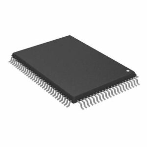
Copy Infineon Locked MCU MB90F342CAPFR-G Flash Heximal to new microcontroller, unlock fujitsu MB90F342CAP secured microcontroller flash memory and clone MB90F342E flash firmware to new microprocessor;
The recommended operating conditions are required in order to ensure the normal operation of the semiconductor device. All of the device’s electrical characteristics are warranted when the device is operated within these ranges.
Always use semiconductor devices within their recommended operating condition ranges. Operation outside these ranges may adversely affect reliability and could result in device failure.
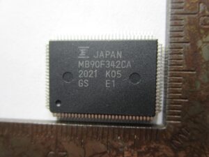
Copiez le micrologiciel intégré flash INFINEON verrouillé MCU MB90F342CAPFR-G des données heximales ou du fichier binaire sur le nouveau microcontrôleur, déverrouillez la mémoire flash sécurisée du microprocesseur FUJITSU MB90F342CAP et répliquez le programme MB90F342E sur une nouvelle unité clonée par microprocesseur ;
No warranty is made with respect to uses, operating conditions, or combinations not represented on the data sheet. Users considering application outside the listed conditions are advised to contact their FUJITSU representatives beforehand.
The oscillation time of the oscillator is the time it takes for the amplitude of the oscillations to reach 90%. For crystal oscillators, this time is between several ms and several tens of ms to reverse engineering MB90F345CA microcontroller flash memory, for ceramic oscillators the time is between several hundred ms and several ms, and for an external clock, the time is 0 ms.
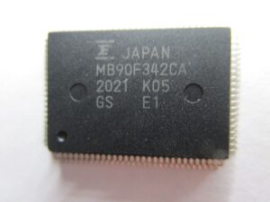
Kopieren Sie die von INFINEON gesperrte MCU MB90F342CAPFR-G-Flash-eingebettete Firmware von Heximaldaten oder Binärdateien auf den neuen Mikrocontroller, entsperren Sie den FUJITSU MB90F342CAP-gesicherten Mikroprozessor-Flash-Speicher und replizieren Sie das MB90F342E-Programm auf die neue geklonte Mikroprozessoreinheit;
Resolution : Analog variation that is recognized by the A/D converter.
Non linearity error
Differential linearity error : The deviation between the actual conversion characteristics and a line that joins the
zero-transition line ( “00 0000 0000” ¬ ® “00 0000 0001” ) to the full-scale transition line
( “11 1111 1110” ¬ ® “11 1111 1111” ) . : Deviation of input voltage, which is required for changing output code by 1 LSB, from an ideal value.
Use the device with external circuits of the following output impedance for analog inputs :
Recommended output impedance of external circuits are : Approx. 1.5 kL or lower (4.0 V £ AVCC £ 5.5 V,
sampling period = 0.5 ms)
 Restoring Infineon MB90F342APFV-G MCU Flash Firmware
Restoring Infineon MB90F342APFV-G MCU Flash Firmware needs to unlock Fujitsu MB90F342ES microcontroller secured IC flash memory and then dump flash memory binary to new microcontroller MB90F342APFV;
Restoring Infineon MB90F342APFV-G MCU Flash Firmware needs to unlock Fujitsu MB90F342ES microcontroller secured IC flash memory and then dump flash memory binary to new microcontroller MB90F342APFV;
This parameter is based on VSS = AVSS = 0 V
*2: Set AVCC and VCC to the same voltage. Make sure that AVCC does not exceed VCC and that the voltage at the analog inputs does not exceed AVCC when the power is switched on.
*3: VI and VO should not exceed VCC + 0.3 V. VI should not exceed the specified ratings. However if the maximum current to/from an input is limited by some means with external components, the ICLAMP rating supersedes the VI rating.
*4: Applicable to pins: P00 to P07, P10 to P17, P20 to P27, P30 to P37, P40 to P47, P50 to P57, P60 to P67, P70 to P77, P80 to P87, P90 to P97, PA0, PA1
*5: · Applicable to pins: P00 to P07, P10 to P17, P20 to P27, P30 to P37, P40 to P47,
відновлення вбудованої прошивки флеш-пам’яті INFINEON MB90F342APFV-G із заблокованим MCU потрібно зламати флеш-пам’ять мікроконтролера FUJITSU MB90F342ES, а потім витягти двійковий код або шістнадцяткові дані на новий мікропроцесор MB90F342APFV
P50 to P57 (Evaluation device : P50 to P55) , P60 to P67, P70 to P77, P80 to P87, P90 to P97, PA0 to PA1
- Use within recommended operating
- Use with DC voltage (current)
- The +B signal should always be applied by using a limiting resistance placed between the +B signal and the
- The value of the limiting resistance should be set so that when the +B signal is applied, the input current to the microcontroller pin does not exceed the rated value, either instantaneously or for prolonged
- Note that when the microcontroller drive current is low, such as in the power saving modes, the +B input
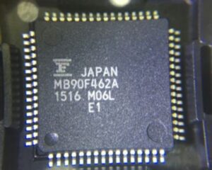
Az INFINEON MB90F342APFV-G zárolt MCU flash beágyazott firmware-ének helyreállításához fel kell törnie a FUJITSU-t MB90F342ES mikrokontrollerrel biztosított IC flash memóriát, majd bináris kódot vagy heximalis adatokat kell kinyernie az új mikroprocesszorba MB90F342APFV
potential may pass through the protective diode and increase the potential at the VCC pin when restoring secured fujitsu MCU MB90F345CAP heximal code, and this may affect other devices.
- Note that if a +B signal is input when the microcontroller power supply is off (not fixed at 0 V) , the power supply is provided from the pins, so that incomplete operation may result.
- Note that if the +B input is applied during power-on, the power supply is provided from the pins and the resulting supply voltage may not be sufficient to operate the power-on reset.
- Care must be taken not to leave the +B input pin
 Recover RH850 R7F7010303AFP Microcontroller Flash Heximal
Recover RH850 R7F7010303AFP Microcontroller Flash Heximal needs to crack R7F7010303AFP renesas locked MCU protection and then pull the embedded firmware out from microprocessor R7F7010303afp flash memory;
Recover RH850 R7F7010303AFP Microcontroller Flash Heximal needs to crack R7F7010303AFP renesas locked MCU protection and then pull the embedded firmware out from microprocessor R7F7010303afp flash memory;
Waveform distortion due to input noise or a reflected wave may cause malfunction. If the input of the CMOS device stays in the area between VIL (MAX) and VIH (MIN) due to noise, etc., the device may malfunction. Take care to prevent chattering noise from entering the device when the input level is fixed when cracking renesas microcontroller R5F563NFDDF flash memory, and also in the transition period when the input level passes through the area between VIL (MAX) and VIH (MIN).
recuperare il programma flash del microcontroller bloccato RH850 R7F7010303AFP nel formato di file binario o dati esimali deve crackare la protezione MCU RENESAS protetta da R7F7010303AFP e quindi estrarre il firmware incorporato dalla memoria flash crittografata del microprocessore RENESAS R7F7010303afp;
Unconnected CMOS device inputs can be cause of malfunction. If an input pin is unconnected, it is possible that an internal input level may be generated due to noise, etc., causing malfunction. CMOS devices behave differently than Bipolar or NMOS devices.
Input levels of CMOS devices must be fixed high or low by using pull-up or pull-down circuitry. Each unused pin should be connected to power supply or GND via a resistor if there is a possibility that it will be an output pin to attack renesas R5F5111FAD mcu flash memory. All handling related to unused pins must be judged separately for each device and according to related specifications governing the device.
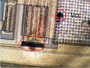
recuperați programul flash de microcontroler blocat RH850 R7F7010303AFP în format de fișier binar sau de date heximale trebuie să spargă protecția MCU RENESAS securizată R7F7010303AFP și apoi scoateți firmware-ul încorporat din memoria flash criptată a microprocesorului RENESAS R7F7010303afp;
 STMicroelectronics ST10F272M-4T3 Locked MCU Flash Content Recovery
STMicroelectronics ST10F272M-4T3 Locked MCU Flash Content Recovery is a process to crack ST10F272M-4T3 secured microcontroller protective fuse bit and copy the embedded software to new microprocessor ST10F272M-4T3;
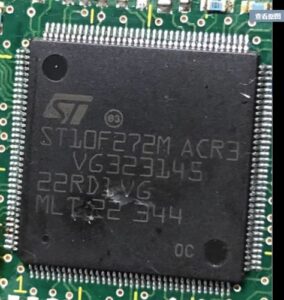
STMicroelectronics ST10F272M-4T3 Locked MCU Flash Content Recovery is a process to crack ST10F272M-4T3 secured microcontroller protective fuse bit and copy the embedded software to new microprocessor ST10F272M-4T3;
CLKOUT function can output either the CPU clock (like in ST10F272M-4T3) or a software programmable prescaled value of the CPU clock. On-chip RAM memory and FLASH size have been increased. PLL multiplication factors have been adapted to new frequency range. A/D Converter is not fully compatible versus ST10F272M-4T3 (timing and programming model). Formula for the conversion time is still valid, while the sampling phase programming model is different.
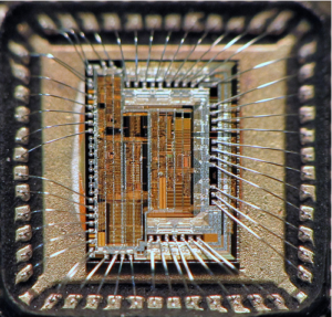
STMicroelectronics ST10F272M locked MCU flash programme recovery – це процес зламу ST10F272M захищеного біта захисного запобіжника мікроконтролера та зчитування вбудованого мікропрограмного забезпечення двійкового коду або шістнадцяткового файлу з оригінальної головної мікросхеми, а потім копіювання вихідного коду на новий мікропроцесор ST10F272M
Besides, additional 8 channels are available on P1L pins as alternate function: The accuracy reachable with these extra channels is reduced with respect to the standard Port5 channels. External Memory bus is affected by limitations on maximum speed and maximum capacitance load: ST10F272m is not able to address an external memory at 64 MHz with 0 wait states in the process of cloning flash memory of locked mcu st10f272m.
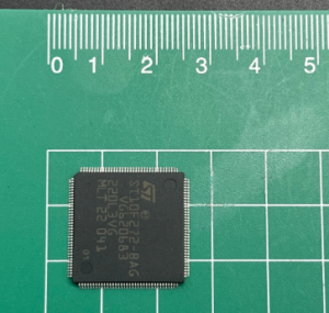
A recuperação do programa flash MCU bloqueado ST10F272M da STMicroelectronics é um processo para quebrar o bit de fusível de proteção do microcontrolador protegido ST10F272M e ler o firmware incorporado do código binário ou arquivo heximal do chip mestre original e depois copiar o código-fonte para o novo microprocessador ST10F272M
XPERCON register bit mapping modified according to new peripherals implementation (not fully compatible with ST10F272m). Bondout chip for emulation (ST10R201) cannot achieve more than 50MHz at room temperature (so no real time emulation possible at maximum speed).
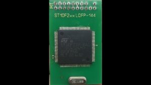
Az STMicroelectronics ST10F272M zárolt MCU flash program helyreállítása egy folyamat az ST10F272M biztonságos mikrokontroller védőbiztosíték bitjének feltörésére és a bináris kód vagy heximális fájl beágyazott firmware-ének kiolvasására az eredeti master chipről, majd a forráskód átmásolására az új ST10F272M mikroprocesszorra
Input section characteristics are different. The threshold programmability is extended to all port pins (additional XPICON register); it is possible to select standard TTL (with up to 400mV of hysteresis) and standard CMOS (with up to 750mV of hysteresis).
 Microchip PIC24FJ32GP203 MCU Flash Memory Heximal Restoration
Microchip PIC24FJ32GP203 MCU Flash Memory Heximal Restoration including unlocking PIC24FJ32GP203 MCU program memory and extract pic24fj32gp203 secured microcontroller flash memory source code;
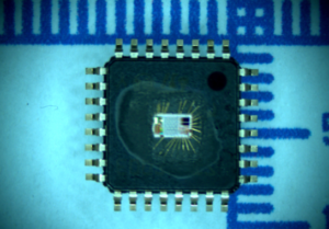
Microchip PIC24FJ32GP203 MCU Flash Memory Heximal Restoration including unlocking PIC24FJ32GP203 MCU program memory and extract pic24fj32gp203 secured microcontroller flash memory source code
In recent years, large value, low-voltage, surface-mount ceramic capacitors have become very cost-effective in sizes up to a few tens of microfarad. The low-ESR, small physical size and other properties make ceramic capacitors very attractive in many types of applications.
Ceramic capacitors are suitable for use with the internal voltage regulator of this microcontroller. However, some care is needed in selecting the capacitor to ensure that it maintains sufficient capacitance over the intended operating range of the application.
Typical low-cost, 10 μF ceramic capacitors are available in X5R, X7R and Y5V dielectric ratings (other types are also available, but are less common). The initial tolerance specifications for these types of capacitors are often specified as ±10% to ±20% (X5R and X7R) or -20%/+80% (Y5V) when breaking pic24fj16ga002 microcontroller flash memory heximal. However, the effective capacitance that these capacitors provide in an application circuit will also vary based on additional factors, such as the applied DC bias voltage and the temperature. The total in-circuit tolerance is, therefore, much wider than the initial tolerance specification.
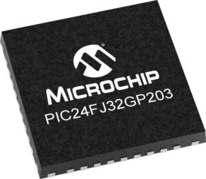
unlock locked microprocessor PIC24FJ32GP203 memory and readout embedded firmware code from microcontroller chip PIC24FJ32GP203 flash memory
The X5R and X7R capacitors typically exhibit satisfactory temperature stability (ex: ±15% over a wide temperature range, but consult the manufacturer’s data sheets for exact specifications). However, Y5V capacitors typically have extreme temperature tolerance specifications of +22%/-82% when recover pic24fj32gp202 mcu flash memory program. Due to the extreme temperature tolerance, a 10 μF nominal rated Y5V type capacitor may not deliver enough total capacitance to meet minimum internal voltage regulator stability and transient response requirements. Therefore, Y5V capacitors are not recommended for use with the internal regulator if the application must operate over a wide temperature range.
 ARM Microcontroller STM32F207IGT6 Flash Firmware Recovery
ARM Microcontroller STM32F207IGT6 Flash Firmware Recovery needs to crack protected MCU STM32F207IGT6 protective system then copy embedded flash content from STM32F207IGT6 MCU memory;
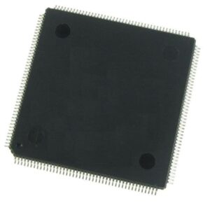
ARM Microcontroller STM32F207IGT6 Flash Firmware Recovery needs to crack protected MCU STM32F207IGT6 protective system then copy embedded flash content from STM32F207IGT6 MCU memory
USART1, USART2, USART3 and USART6 also provide hardware management of the CTS and RTS signals, Smart Card mode (ISO 7816 compliant) and SPI-like communication capability. All interfaces can be served by the DMA controller.
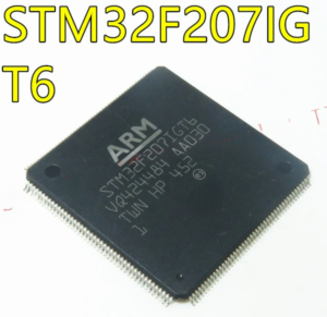
Odzyskiwanie wbudowanego oprogramowania układowego z mikrokontrolerem zabezpieczonym STM32F207IGT6 pamięcią flash ARM musi złamać chroniony system ochronny MCU STM32F207IGT6, a następnie skopiować osadzoną zawartość flash danych binarnych lub programu szesnastkowego z STM32F207IGT6 oryginalnej pamięci mikroprocesora głównego
The STM32F20x devices feature up to three SPIs in slave and master modes in full-duplex and simplex communication modes. SPI1 can communicate at up to 30 Mbits/s, while SPI2 and SPI3 can communicate at up to 15 Mbit/s when breaking arm mcu stm32f205rbt6 flash memory. The 3-bit prescaler gives 8 master mode frequencies and the frame is configurable to 8 bits or 16 bits.
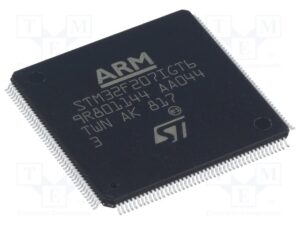
STMicroelectronics STM32F207IGT6 locked mcu fuse bit unlocking and extract embedded firmware heximal program from STMicroelectronics STM32F207IGT6 microprocessor flash memory
The hardware CRC generation/verification supports basic SD Card/MMC modes. All SPIs can be served by the DMA controller. The SPI interface can be configured to operate in TI mode for communications in master mode and slave mode. Two standard I2S interfaces (multiplexed with SPI2 and SPI3) are available. They can operate in master or slave mode, in half-duplex communication modes, and can be configured to operate with a 16-/32-bit resolution as input or output channels.
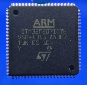
ARM osigurani mikrokontroler STM32F207IGT6 oporavak ugrađenog firmvera mora razbiti zaštićeni MCU STM32F207IGT6 zaštitni sustav, a zatim kopirati ugrađeni flash sadržaj binarnih podataka ili heksimalnog programa iz STM32F207IGT6 izvorne glavne mikroprocesorske memorije
Audio sampling frequencies from 8 kHz up to 192 kHz are supported. When either or both of the I2S interfaces is/are configured in master mode, the master clock can be output to the external DAC/CODEC at 256 times the sampling frequency. All I2Sx interfaces can be served by the DMA controller when recover embedded flash memory content from arm microcontroller stm32f205rct6.
 Clone ARM STM32F205ZFT6 Microcontroller Firmware
Clone ARM STM32F205ZFT6 Microcontroller Firmware needs to readout mcu stmicroelectronics stm32f205zft6 heximal and copy flash memory embedded program to new stm32f205zft6 microprocessor;
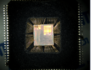
Clone ARM STM32F205ZFT6 Microcontroller Firmware needs to readout mcu stmicroelectronics stm32f205zft6 heximal and copy flash memory embedded program to new stm32f205zft6 microprocessor;
The following conditions must be respected:
- VDD must always be higher than VCAP_1 and VCAP_2 to avoid current injection between power domains (see Figure 8).
- PA0 must be kept low to cover both conditions: until VCAP_1 and VCAP_2 reach 08 V, and until VDD reaches 1.7 V.
- NRST must be controlled by an external reset controller to keep the device under reset when VDD is below 7 V (see Figure 9).
In this mode, when the internal reset is OFF, the following integrated features are no more supported:
- The integrated power-on reset (POR) / power-down reset (PDR) circuitry is
- The brownout reset (BOR) circuitry is
- The embedded programmable voltage detector (PVD) is
VBAT functionality is no more available and VBAT pin must be connected to VDD.
The backup domain of the STM32F20x devices includes:
- The real-time clock (RTC)
- 4 Kbytes of backup SRAM
- 20 backup registers
The real-time clock (RTC) is an independent BCD timer/counter. Its main features are the following:
- Dedicated registers contain the second, minute, hour (in 12/24 hour), week day, date, month, year, in BCD (binary-coded decimal) format.
- Automatic correction for 28, 29 (leap year), 30, and 31 day of the
- Programmable alarm and programmable periodic interrupts with wakeup from Stop and Standby
- It is clocked by a 768 kHz external crystal, resonator or oscillator, the internal low-power RC oscillator or the high-speed external clock divided by 128 will recover arm microcontroller stm32f205rg flash code. The internal low-speed RC has a typical frequency of 32 kHz. The RTC can be calibrated using an external 512 Hz output to compensate for any natural quartz deviation.
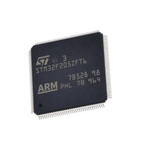
clone locked mcu chip STM32F205ZFT6 flash memory content after crack STM32F205ZFT6 microcontroller fuse bit
- Two alarm registers are used to generate an alarm at a specific time and calendar fields can be independently masked for alarm comparison. To generate a periodic interrupt, a 16-bit programmable binary auto-reload downcounter with programmable resolution is available and allows automatic wakeup and periodic alarms from every 120 µs to every 36 hours when attacking stmicroelectronics stm32f205vb mcu protection.
- A 20-bit prescaler is used for the time base It is by default configured to generate a time base of 1 second from a clock at 32.768 kHz.
- Reference clock detection: a more precise second source clock (50 or 60 Hz) can be used to enhance the calendar
 Locked MCU Chip STM32F205ZCT6 Program Restoration
Locked MCU Chip STM32F205ZCT6 Program Restoration needs to crack stm32f205zct6 processor protective resistance system firstly then extract stm32f205zct6 microcontroller flash memory content;
Locked MCU Chip STM32F205ZCT6 Program Restoration needs to crack stm32f205zct6 processor protective resistance system firstly then extract stm32f205zct6 microcontroller flash memory content
This feature is available only on packages featuring the REGOFF pin. The regulator is disabled by holding REGOFF high. The regulator OFF mode allows to supply externally a V12 voltage source through VCAP_1 and VCAP_2 pins.
The two 2.2 µF ceramic capacitors must be replaced by two 100 nF decoupling capacitors. Refer to Figure 19: Power supply scheme.
When the regulator is OFF, there is no more internal monitoring on V12. An external power supply supervisor must be used to monitor the V12 of the logic power domain when breaking stm32f205rb flash memory protection. PA0 pin must be used for this purpose, and act as power-on reset on V12 power domain.
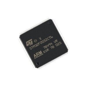
crack locked mcu chip STM32F205ZCT6 and copy embedded heximal firmware from microcontroller STM32F205ZCT6 flash memory
In regulator OFF mode, the following features are no more supported:
- PA0 cannot be used as a GPIO pin since it allows to reset the part of the 2 V logic power domain which is not reset by the NRST pin.
- As long as PA0 is kept low, the debug mode cannot be used at power-on As a consequence, PA0 and NRST pins must be managed separately if the debug connection at reset or pre-reset is required.
Regulator OFF / internal reset ON
On WLCSP64+2 package, this mode is activated by connecting REGOFF pin to VDD and IRROFF pin to VSS. On UFBGA176 package, only REGOFF must be connected to VDD (IRROFF not available). In this mode, VDD/VDDA minimum value is 1.8 V to recover stm32f205rc microcontroller flash memory heximal.
The regulator OFF / internal reset ON mode allows the user to supply externally a 1.2 V voltage source through VCAP_1 and VCAP_2 pins, in addition to VDD.
 Restoring ARM STM32F205RE MCU Flash Firmware
Restoring ARM STM32F205RE MCU Flash Firmware starts from decrypt ARM STM32F205RE microcontroller flash memory program and then readout embedded code from microprocessor stm32f205re flash memory;
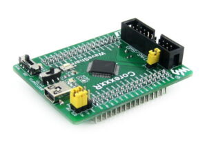
Restoring ARM STM32F205RE MCU Flash Firmware starts from decrypt ARM STM32F205RE microcontroller flash memory program and then readout embedded code from microprocessor stm32f205re flash memory
For the LQFP100 package, only FSMC Bank1 or Bank2 are Bank1 can only support a multiplexed NOR/PSRAM memory using the NE1 Chip Select. Bank2 can only support a 16- or 8-bit NAND Flash memory using the NCE2 Chip Select. The interrupt line cannot be used since Port G is not available in this package.
The SPI2 and SPI3 interfaces give the flexibility to work in an exclusive way in either the SPI mode or the I2S audio on devices in WLCSP64+2 package for arm stm32f205rc mcu flash memory heximal recovery, if IRROFF is set to VDD, the supply voltage can drop to 7 V when the device operates in the 0 to 70 °C temperature range using an external power supply supervisor.
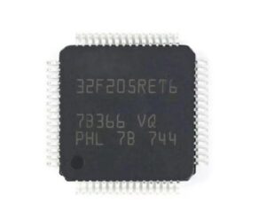
взломать защищенный mcu stm32f205ret6 и скопировать программу flash heximal memory из прошивки микропроцессора stm32f205ret6
The STM32F205xx constitute the STM32F20x family, whose members are fully pin-to-pin, software and feature compatible, allowing the user to try different memory densities and peripherals for a greater degree of freedom during the development cycle.
The STM32F205xx and STM32F207xx devices maintain a close compatibility with the whole STM32F10xxx family. All functional pins are pin-to-pin compatible. The STM32F205xx and STM32F207xx, however, are not drop-in replacements for the STM32F10xxx devices: the two families do not have the same power scheme, and so their power pins are different. Nonetheless, transition from the STM32F10xxx to the STM32F20x family remains simple as only a few pins are impacted.