Archive for the ‘Break IC’ Category
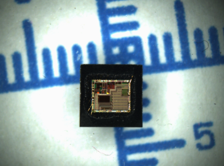
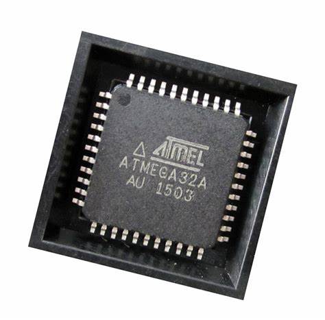
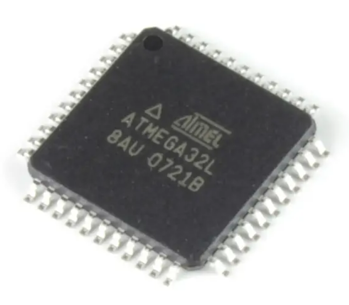
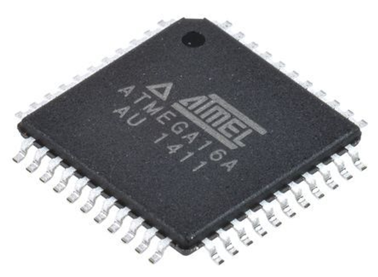
 Breaking Encrypted ATMEGA32A MCU Flash
Breaking Encrypted ATMEGA32A MCU Flash and pull microcontroller atmega32a firmware out from its flash and eeprom memory, the software file of atmega32a atmel chip can be readout directly by programmer after reset the fuse bit;
EEPROM data corruption can easily be avoided by following this design recommendation: Keep the AVR RESET active (low) during periods of insufficient power supply voltage. This can be done by enabling the internal Brown-out Detector (BOD).
If the detection level of the internal BOD does not match the needed detection level, an external low VCC Reset Protection circuit can be used. If a reset occurs while a write operation is in progress of breaking atmega16l locked mcu flash memory, the write operation will be completed provided that the power supply voltage is sufficient.
quebrando o flash criptografado ATMEGA32A MCU e puxar o microcontrolador atmega32a firmware para fora de sua memória flash e eeprom, o arquivo de software do chip atmega32a atmel pode ser lido diretamente pelo programador após a redefinição do bit de fusível;
Below Figure presents the principal clock systems in the AVR and their distribution. All of the clocks need not be active at a given time. In order to reduce power consumption, the clocks to modules not being used can be halted by using different sleep modes, as described in “Power Management and Sleep Modes” on page 39. The clock systems are detailed below Figure.
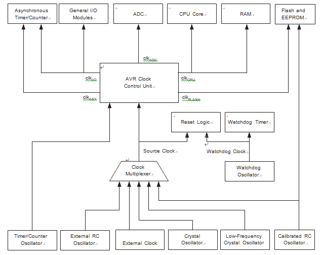
The CPU clock is routed to parts of the system concerned with operation of the AVR core. Examples of such mod- ules are the General Purpose Register File by recover atmega16 microprocessor firmware, the Status Register and the Data memory holding the Stack Pointer. Halting the CPU clock inhibits the core from performing general operations and calculations.
Restoring ATmega32L Microprocessor Memory Software
Restoring ATmega32L Microprocessor Memory Software in the format of heximal or binary, original memory data inside atmega32l mcu will be cloned and embedded firmware will be readout from atmega32l;
The EEPROM Write Enable Signal EEWE is the write strobe to the EEPROM. When address and data are correctly set up, the EEWE bit must be written to one to write the value into the EEPROM. The EEMWE bit must be written to one before a logical one is written to EEWE, otherwise no EEPROM write takes place. The following pro- cedure should be followed when writing the EEPROM (the order of steps 3 and 4 is not essential):
- Wait until EEWE becomes zero.
- Wait until SPMEN in SPMCR becomes zero.
- Write new EEPROM address to EEAR (optional).
- Write new EEPROM data to EEDR (optional).
- Write a logical one to the EEMWE bit while writing a zero to EEWE in EECR.
- Within four clock cycles after setting EEMWE, write a logical one to EEWE.
The EEPROM can not be programmed during a CPU write to the Flash memory. The software must check that the Flash programming is completed before initiating a new EEPROM write to reverse engineer atmega8a microchip memory. Step 2 is only relevant if the software con- tains a boot loader allowing the CPU to program the Flash.
If the Flash is never being updated by the CPU, step 2 can be omitted. See “Boot Loader Support – Read-While-Write Self-Programming” on page 201 for details about boot programming.
Caution: An interrupt between step 5 and step 6 will make the write cycle fail, since the EEPROM Master Write Enable will time-out. If an interrupt routine accessing the EEPROM is interrupting another EEPROM access.
restaurando o software de memória do microprocessador ATmega32L no formato de heximal ou binário, os dados de memória originais dentro do atmega32l mcu serão clonados e o firmware incorporado será lido a partir do atmega32
the EEAR or EEDR Register will be modified, causing the interrupted EEPROM access to fail. It is recommended to have the Global Interrupt Flag cleared during all the steps to avoid these problems.
When the write access time has elapsed, the EEWE bit is cleared by hardware in order to restore microcontroller atmega8l flash data. The user software can poll this bit and wait for a zero before writing the next byte. When EEWE has been set, the CPU is halted for two cycles before the next instruction is executed.
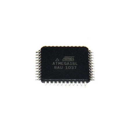
Break ATmega16L Locked MCU Flash Memory
Break ATmega16L Locked MCU Flash Memory and copy heximal code to new atmega16l microprocessor, after extract embedded firmware from microcontroller atmega16l;
The Microchip AVR® ATmega8A contains 512 bytes of data EEPROM memory. It is organized as a separate data space, in which single bytes can be read and written.
The EEPROM has an endurance of at least 100,000 write/erase cycles. The access between the EEPROM and the CPU is described bellow, specifying the EEPROM Address Registers when crack atmega16a microcontroller flash memory, the EEPROM Data Register, and the EEPROM Control Register.
The EEPROM Access Registers are accessible in the I/O space.
The write access time for the EEPROM is given in Table 8-1 on page 27. A self-timing function, however, lets the user software detect when the next byte can be written.
quebrar ATmega16L bloqueado MCU memória flash e copiar código heximal para o novo microprocessador atmega16l, após extrair firmware incorporado do microcontrolador atmega16l
If the user code contains instructions that write the EEPROM, some precautions must be taken in order to recover atmega16 microprocessor firmware. In heavily filtered power supplies, VCC is likely to rise or fall slowly on
Power-up/down. This causes the device for some period of time to run at a voltage lower than specified as mini- mum for the clock frequency used.
Cracking ATmega16A Microcontroller Flash Memory
Cracking ATmega16A Microcontroller Flash Memory is a process to break atmega16a mcu fuse bit, readout heximal file from microprocessor atmega16a avr chip;
When the AVR exits from an interrupt, it will always return to the main program and execute one more instruction before any pending interrupt is served.
Note that the Status Register is not automatically stored when entering an interrupt routine, nor restored when returning from an interrupt routine. This must be handled by software.
When using the CLI instruction to disable interrupts, the interrupts will be immediately disabled. No interrupt will be executed after the CLI instruction, even if it occurs simultaneously with the CLI instruction.
The following example shows how this can be used to avoid interrupts during the timed EEPROM write sequence by attacking mcu atmega162 flash memory.
rachadura ATmega16A memória flash microcontrolador é um processo para quebrar atmega16a mcu bit fusível, arquivo heximal de leitura do microprocessador atmega16a avr chip
When using the SEI instruction to enable interrupts, the instruction following SEI will be executed before any pend- ing interrupts, as shown in the following example.
The interrupt execution response for all the enabled Microchip AVR® interrupts is four clock cycles minimum. After four clock cycles, the Program Vector address for the actual interrupt handling routine is executed by break mcu atmega16a flash memory. During this 4- clock cycle period, the Program Counter is pushed onto the Stack.
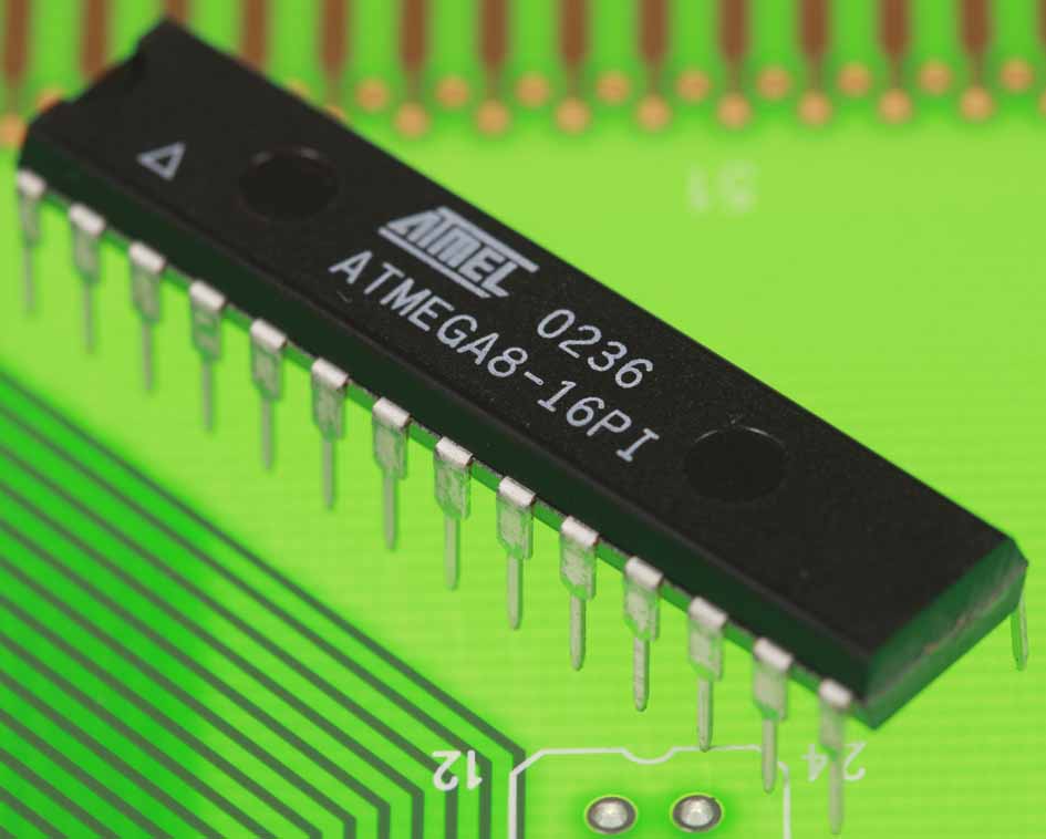
Microchip ATmega8 MCU Flash Content Pulling
Microchip ATmega8 MCU Flash Content Pulling will help engineer to copy avr mcu atmega8 microcontroller heximal from its flash memory, and then extract atmega8 chip binary;
The ALU supports arithmetic and logic operations between registers or between a constant and a register. Single register operations can also be executed in the ALU. After an arithmetic operation, the Status Register is updated to reflect information about the result of the operation.
The Program flow is provided by conditional and unconditional jump and call instructions, able to directly address the whole address space. Most AVR instructions have a single 16-bit word format to reverse engineering atmel microchip atmega8l firmware. Every Program memory address contains a 16- or 32-bit instruction.
Microchip ATmega8 MCU flash conteúdo puxando ajudará o engenheiro a copiar avr mcu atmega8 microcontrolador heximal de sua memória flash e, em seguida, extrair atmega8 chip binário
Program Flash memory space is divided in two sections, the Boot program section and the Application program section. Both sections have dedicated Lock Bits for write and read/write protection.
The SPM instruction that writes into the Application Flash memory section must reside in the Boot program section to copy ic atmega8l heximal file. During interrupts and subroutine calls, the return address Program Counter (PC) is stored on the Stack .
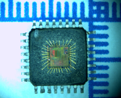
Attack Renesas R5F21244SDFP Microcontroller Protection
Attack Renesas R5F21244SDFP Microcontroller Protection and unlock microprocessor r5f21244sd flash memory, extract embedded heximal file from MCU memory;
- The measurement condition is Topr = -20 to 85°C (N version) / -40 to 85°C (D version), unless otherwise specified.
- 2. This condition (external power VCC rise gradient) does not apply if VCC ³ 1.0 V.
To use the power-on reset function, enable voltage monitor 0 reset by setting the LVD0ON bit in the OFS register to 0, the VW0C0 and VW0C6 bits in the VW0C register to 1 respectively by copying locked r5f212dasn mcu flash data, and the VCA25 bit in the VCA2 register to 1.
- When using the voltage monitor 0 digital filter, ensure that the voltage is within the MCU operation voltage range (2.2 V or above) during the sampling time.
- The sampling clock can be selected. Refer to 6. Voltage Detection Circuit of Hardware Manual for details.
Vdet0 indicates the voltage detection level of the voltage detection 0 circuit. Refer to 6. Voltage Detection Circuit of Hardware Manual for details
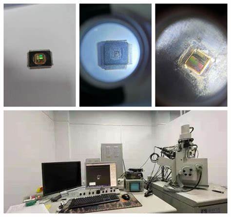
atacar Renesas R5F21244SDFP microcontrolador Proteção e desbloquear microprocessador r5f21244sd memória flash, extrair arquivo heximal incorporado da memória MCU;
- VCC = 2.2 to 5.5 V, Topr = -20 to 85°C (N version) / -40 to 85°C (D version), unless otherwise specified.
- 2. Standard values when the FRA1 register value after reset is assumed.
- 3. Standard values when the corrected value of the FRA6 register has been written to the FRA1 register when copying locked r5f212aasd microcontroller memory data.
This enables the setting errors of bit rates such as 9600 bps and 38400 bps to be 0% when the serial interface is used in UART mode.
Break R5F21292SDSP Locked MCU Flash Memory
Break R5F21292SDSP Locked MCU Flash Memory and clone microcontroller r5f21292 heximal file to new units which will provide the same functions as original ones;
VCC = 2.7 to 5.5 V at Topr = -20 to 85°C (N version) / -40 to 85°C (D version), unless otherwise specified.
The programming and erasure endurance is defined on a per-block basis.
If the programming and erasure endurance is n (n = 100 or 10,000), each block can be erased n times. For example, if 1,024 1-byte writes are performed to block A, a 1 Kbyte block, and then the block is erased, the programming/erasure endurance still stands at one.
However, the same address must not be programmed more than once per erase operation (overwriting prohibited).
Endurance to guarantee all electrical characteristics after program and erase. (1 to Min. value can be guaranteed).
Standard of block A and block B when program and erase endurance exceeds 1,000 times. Byte program time to 1,000 times is the same as that in program ROM.
quebrar R5F21292SDSP bloqueado MCU memória flash e clone microcontrolador r5f21292 arquivo heximal para novas unidades que irá fornecer as mesmas funções que os originais;
In a system that executes multiple programming operations, the actual erasure count can be reduced by writing to sequential addresses in turn so that as much of the block as possible is used up before performing an erase operation. For example, when programming groups of 16 bytes, the effective number of rewrites can be minimized by programming up to 128 groups before erasing them all in one operation.
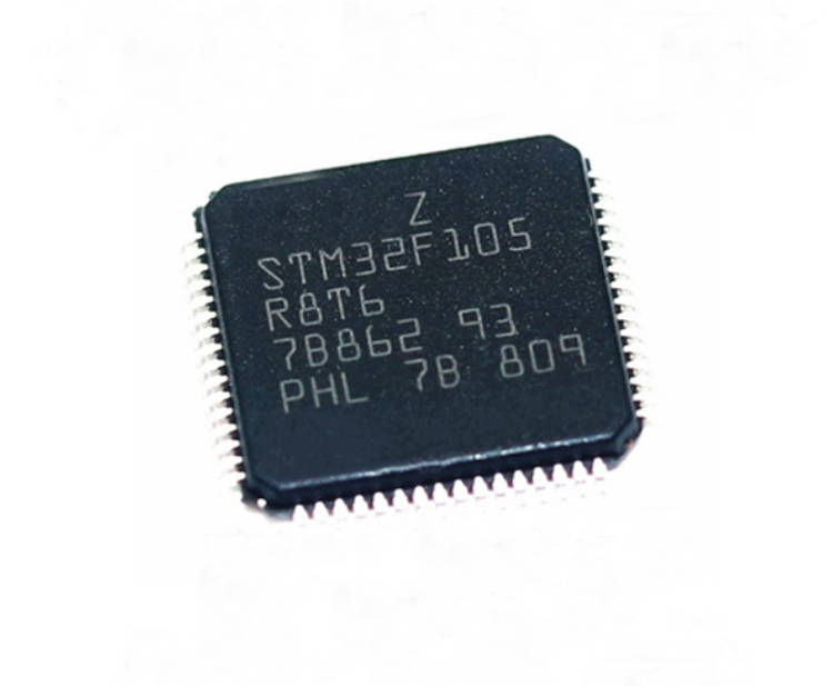
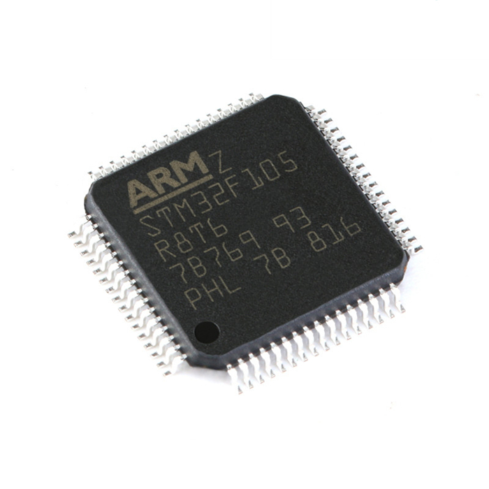
Unlock STM32F105R8 Secured Microprocessor Flash Memory
Unlock STM32F105R8 Secured Microprocessor Flash Memory and extract embedded firmware from locked MCU STM32F105R8, and then copy heximal file to new stm32f105r8 microcontroller;

The STM32F050xx family supports three low-power modes to achieve the best compromise between low power consumption, short startup time and available wakeup sources:
● Sleep mode
In Sleep mode, only the CPU is stopped. All peripherals continue to operate and can wake up the CPU when an interrupt/event occurs.
● Stop mode
Stop mode achieves very low power consumption while retaining the content of SRAM and registers. All clocks in the 1.8 V domain are stopped, the PLL, the HSI RC and the HSE crystal oscillators are disabled in order to replicating embedded flash program from stm32f105r8 mcu. The voltage regulator can also be put either in normal or in low power mode.
crack locked stm32f105r8 MCU fuse bit and restore embedded heximal program file from flash memory of stm32f105r8 MCU
The device can be woken up from Stop mode by any of the EXTI lines. The EXTI line source can be one of the 16 external lines, the PVD output, RTC alarm, I2C1 or USART1.
The I2C1 and the USART1 can be configured to enable the HSI RC oscillator for processing incoming data. If this is used, the voltage regulator should not be put in the low-power mode but kept in normal mode.
● Standby mode
The Standby mode is used to achieve the lowest power consumption. The internal voltage regulator is switched off so that the entire 1.8 V domain is powered off. The PLL, the HSI RC and the HSE crystal oscillators are also switched off. After entering Standby mode for the sake of restoring arm microcontroller stm32f103c4 flash binary, SRAM and register contents are lost except for registers in the Backup domain and Standby circuitry.
attack encrypted stm32f105r8t6 microcontroller protection and copy heximal program software from flash memory
The device exits Standby mode when an external reset (NRST pin), a IWDG reset, a rising edge on the WKUP pins, or an RTC alarm occurs.
Note: The RTC, the IWDG, and the corresponding clock sources are not stopped by entering Stop or Standby mode.
Dump Renesas R5F212A7SDFA Protect MCU Flash Program
Dump Renesas R5F212A7SDFA Protect MCU Flash Program needs to know its internal structure and programming mechanism, extract its embedded firmware from R5F212A7SDFA microcontroller, and clone heximal file to new microprocessor R5F212A7SDFA;

R8C/Tiny series core
- Number of fundamental instructions: 89
- Minimum instruction execution time:
50 ns (f(XIN) = 20 MHz, VCC = 3.0 to 5.5 V)
100 ns (f(XIN) = 10 MHz, VCC = 2.7 to 5.5 V)
200 ns (f(XIN) = 5 MHz, VCC = 2.2 to 5.5 V)
- Multiplier: 16 bits × 16 bits ® 32 bits
- Multiply-accumulate instruction: 16 bits × 16 bits + 32 bits ® 32 bits
Operation mode: Single-chip mode (address space: 1 Mbyte)
3 circuits: XIN clock oscillation circuit (with on-chip feedback resistor) to breaking mcu R5F2L388 flash firmware,
On-chip oscillator (high-speed, low-speed)
(high-speed on-chip oscillator has a frequency adjustment function), XCIN clock oscillation circuit (32 kHz)
- Oscillation stop detection: XIN clock oscillation stop detection function
- Frequency divider circuit: Dividing selectable 1, 2, 4, 8, and 16
- Low power consumption modes:
Standard operating mode (high-speed clock, low-speed clock, high-speed on-chip oscillator, low-speed on-chip oscillator), wait mode, stop mode.
dump Renesas R5F212A7SDFA protegido MCU flash programa precisa conhecer sua estrutura interna e mecanismo de programação, extrair seu firmware incorporado do microcontrolador R5F212A7SDFA e clonar o arquivo heximal para o novo microprocessador R5F212A7SDFA
- External: 5 sources, Internal: 23 sources, Software: 4 sources
Priority levels: 7 levels
8 bits × 1 (with 8-bit prescaler)
Timer mode (period timer), pulse output mode (output level inverted every period), event counter mode, pulse width measurement mode, pulse period measurement mode.
8 bits × 1 (with 8-bit prescaler)
Timer mode (period timer), programmable waveform generation mode (PWM output), programmable one-shot generation mode, programmable wait one- shot generation mode
Breaking MCU STM32F050G4 Flash Memory
Breaking MCU STM32F050G4 Flash Memory and extract embedded heximal file out from microcontroller stm32f050g4, copy firmware from original microprocessor stm32f050g4 flash memory;
These features make the STM32F050xx microcontroller family suitable for a wide range of applications such as control application and user interfaces, handheld equipment, A/V receivers and digital TV, PC peripherals, gaming and GPS platforms, industrial applications, PLCs, inverters, printers, scanners, alarm systems, video intercoms, and HVACs.
The ARM Cortex™-M0 processor is the latest generation of ARM processors for embedded systems which will be used for reverse engineering stm32f078vb microcontroller. It has been developed to provide a low-cost platform that meets the needs of MCU implementation, with a reduced pin count and low-power consumption, while delivering outstanding computational performance and an advanced system response to interrupts.
quebrando a memória flash MCU STM32F050G4 e extrair arquivo heximal embutido do microcontrolador stm32f050g4, copiar firmware do microprocessador original stm32f050g4 memória flash;
The ARM Cortex™-M0 32-bit RISC processor features exceptional code-efficiency, delivering the high-performance expected from an ARM core in the memory size usually associated with 8- and 16-bit devices for recovering stm32f051c4 microcontroller flash binary. The STM32F050xx family has an embedded ARM core and is therefore compatible with all ARM tools and software.