Archive for the ‘Break IC’ Category
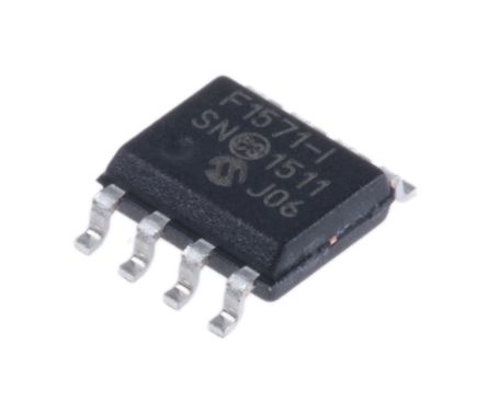
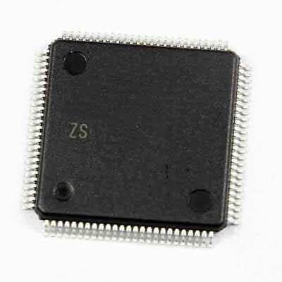
 Break Microchip PIC12F1571 MCU Protection
Break Microchip PIC12F1571 MCU Protection and read embedded firmware out from pic12f1571 microcontroller flash and eeprom memory, and then clone heximal program to new microprocessor PIC12F1571;
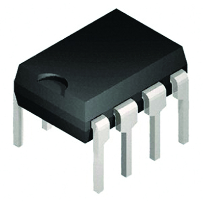
Break Microchip PIC12F1571 MCU Protection and read embedded firmware out from pic12f1571 microcontroller flash and eeprom memory, and then clone heximal program to new microprocessor PIC12F1571
PIC12F1257 microcontrollers combine the capabilities of 16-bit PWMs with Analog to suit a variety of applications. These devices deliver four 16-bit PWMs with independent timers for applications where high resolution is needed, such as LED lighting, stepper motors, power supplies and other general purpose applications which is useful.
The core independent peripherals (16-bit PWMs, Complementary Waveform Generator), Enhanced Universal Synchronous Asynchronous Receiver Transceiver (EUSART) and Analog (ADCs, Comparator and DAC) enable closed-loop feedback and communication for use in multiple market segments to restoring pic16f870 mcu heximal code.
The Peripheral Pin Select (PPS) functionality allows for I/O pin remapping of the digital peripherals for increased flexibility. The EUSART peripheral enables the communication for applications such as LIN.
Сломайте защиту микроконтроллера Microchip PIC12F1571 и прочитайте встроенную прошивку из флэш-памяти микроконтроллера pic12f1571 и памяти eeprom, а затем клонируйте шестнадцатеричную программу в новый микропроцессор PIC12F1571.
For the A/D converter to meet its specified accuracy, the charge holding capacitor (CHOLD) must be allowed to fully charge to the input channel voltage level. The analog input model is shown in Figure 17-2. The source impedance (RS) and the internal sampling switch (RSS) impedance directly affect the time required to charge the capacitor CHOLD by extracting mcu pic18f2520 embedded firmware.
The sampling switch (RSS) impedance varies over the device voltage (VDD). The source impedance affects the offset voltage at the analog input (due to pin leakage current). The maximum recommended impedance for analog sources is 2.5 kW. After the analog input channel is selected (changed), the channel must be sampled for at least the minimum acquisition time before starting a conversion.
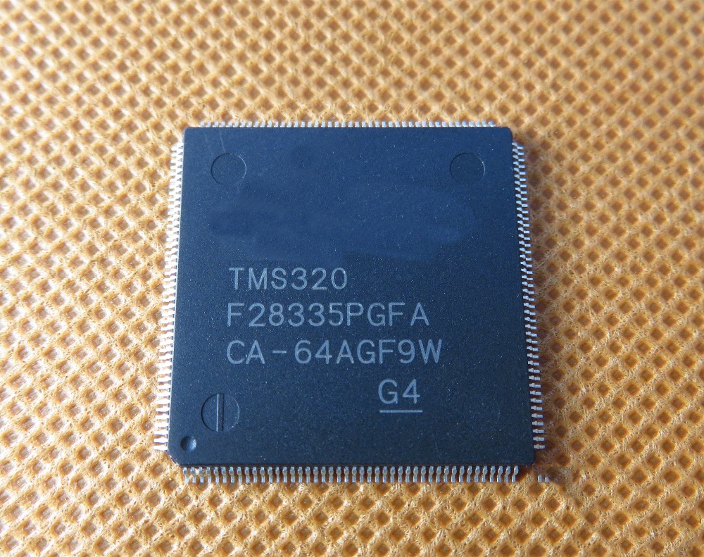
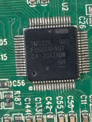
Break DSP TMS320F2810PBKS Microcontroller Locked Memory
Break DSP TMS320F2810PBKS Microcontroller Locked Memory and extract mcu tms320f2810pb flash memory content, original embedded firmware will be restored from microprocessor tms320f2810pb dsp mcu;
The 2803x devices incorporate a method to reduce the device current consumption. Because each peripheral unit has an individual clock-enable bit, significant reduction in current consumption can be achieved by turning off the clock to any peripheral module that is not used in a given application.
romper DSP TMS320F2810PBKS microcontrolador bloqueado la memoria y extraer mcu tms320f2810pb contenido de la memoria flash, el firmware original incrustado será restaurado desde el microprocesador tms320f2810pb dsp mcu
Furthermore, any one of the three low-power modes could be taken advantage of to reduce the current consumption even further to attack ic mcu tms320f28232pg software. Below Table indicates the typical reduction in current consumption achieved by turning off the clocks.
All peripheral clocks (except CPU Timer clock) are disabled upon reset. Writing to/reading from peripheral registers is possible only after the peripheral clocks are turned on.
This number represents the current drawn by the digital portion of the ADC module to recover microcontroller tms320f2812pg firmware. Turning off the clock to the ADC module results in the elimination of the current drawn by the analog portion of the ADC (IDDA) as well.
For peripherals with multiple instances, the current quoted is per module. For example, the 2 mA value quoted for ePWM is for one ePWM module.
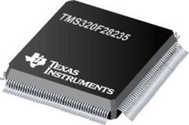
Attack TMS320F28235PG Microprocessor Protection System
Attack TMS320F28235PG Microprocessor Protection System and restore embedded binary file from mcu tms320f28235pg mcu flash memory;
If glitching is unacceptable in an application, 1.8 V could be supplied externally. Alternatively, adding a current-limiting resistor (for example, 470 Ω) in series with these pins and any external driver could be considered to limit the potential for degradation to the pin and/or external circuitry.
atacar el sistema de protección del microprocesador TMS320F28235PG y restaurar el archivo binario embebido de la memoria flash mcu tms320f28235pg mcu;
There is no power-sequencing requirement when using an external 1.8-V supply. However, if the 3.3-V transistors in the level-shifting output buffers of the I/O pins are powered before the 1.8-V transistors when extract texas instrument mcu tms320f2812pg code, it is possible for the output buffers to turn on, causing a glitch to occur on the pin during power up.
To avoid this behavior, power the VDD pins before or with the VDDIO pins, ensuring that the VDD pins have reached 0.7 V before the VDDIO pins reach 0.7 V.
The peripheral – I/O multiplexing implemented in the device prevents all available peripherals from being used at the same time. This is because more than one peripheral function may share an I/O pin to crack ti microcontroller tms320f28032 flash memory. It is, however, possible to turn on the clocks to all the peripherals at the same time, although such a configuration is not useful. If this is done, the current drawn by the device will be more than the numbers specified in the current consumption tables.
Texas Instruments TMS320F28034PNQ MCU Breaking
Texas Instruments TMS320F28034PNQ MCU Breaking is a process to unlock tms320f28034pnq controller’s flash memory and then readout embedded data from microcontroller tms320f28034pnq;

Section 6.2.1 describes the signals. With the exception of the JTAG pins, the GPIO function is the default at reset, unless otherwise mentioned. The peripheral signals that are listed under them are alternate functions. Some peripheral functions may not be available in all devices.
See Table 5-1 for details. Inputs are not 5-V tolerant. All GPIO pins are I/O/Z and have an internal pullup when reverse engineering dsp mcu tms320f28034 flash memory, which can be selectively enabled/disabled on a per-pin basis. This feature only applies to the GPIO pins.
Texas Instruments TMS320F28034PNQ MCU romper es un proceso para desbloquear tms320f28034pnq memoria flash del controlador y luego leer los datos incrustados de tms320f28034pnq microcontrolador;
The pullups on the PWM pins are not enabled at reset. The pullups on other GPIO pins are enabled upon reset. The AIO pins do not have an internal pullup.
When the on-chip VREG is used, the GPIO19, GPIO34, GPIO35, GPIO36, GPIO37, and GPIO38 pins could glitch during power up in order to recover secured dsp tms320f28035 microcontroller flash controller. This potential glitch will finish before the boot mode pins are read and will not affect boot behavior.
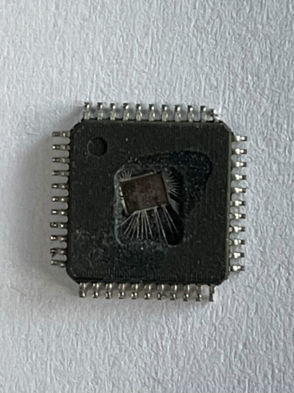
Break Secured STM32F091CB MCU Flash Memory
Break Secured STM32F091CB MCU Flash Memory and extract embedded source code from stm32f091cb microcontroller flash memory, the binary program inside stm32f091cb microprocessor will be copied;
One standard I2S interface (multiplexed with SPI1) supporting four different audio standards can operate as master or slave at half-duplex communication mode. It can be configured to transfer 16 and 24 or 32 bits with16-bit or 32-bit data resolution and synchronized by a specific signal.
Audio sampling frequency from 8 kHz up to 192 kHz can be set by 8-bit programmable linear prescaler. When operating in master mode it can output a clock for an external audio component at 256 times the sampling frequency when recover flash binary from stm32f051c4 microcontroller.
An ARM SW-DP interface is provided to allow a serial wire debugging tool to be connected to the MCU.
PC13, PC14 and PC15 are supplied through the power switch. Since the switch only sinks a limited amount of current (3 mA), the use of GPIO PC13 to PC15 in output mode is limited: The speed should not exceed 2 MHz with a maximum load of 30 pF these GPIOs must not be used as a current sources (e.g. to drive an LED).
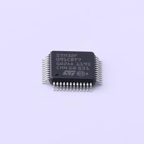
romper la memoria flash asegurada STM32F091CB MCU y extraer el código fuente embebido de la memoria flash del microcontrolador stm32f091cb, se copiará el programa binario dentro del microprocesador stm32f091cb;
After the first backup domain power-up, PC13, PC14 and PC15 operate as GPIOs. Their function then depends on the content of the Backup registers which is not reset by the main reset.
For details on how to manage these GPIOs, refer to the Battery backup domain and BKP register description sections in the STM32F05xx reference manual to restoring stm32f051c6 microprocessor flash heximal. This alternate feature is available on standard dies only.
After reset, these pins are configured as SWDAT and SWCLK alternate functions, and the internal pull-up on SWDAT pin and internal pull-down on SWCLK pin are activated.
Attack Microchip PIC18F45K40T Controller Memory
Attack Microchip PIC18F45K40T Controller Memory is a process to unlock microcontroller pic18f45k40t security fuse bit, and then readout flash memory software from microprocessor pic18f45k40t chipset;
On boards with power traces running longer than six inches in length, it is suggested to use a tank capac- itor for integrated circuits, including microcontrollers, to supply a local power source.
The value of the tank capacitor should be determined based on the trace resistance that connects the power supply source to the device, and the maximum current drawn by the device in the application. In other words, select the tank capacitor so that it meets the acceptable voltage sag at the device. Typical values range from 4.7 mF to 47 mF.
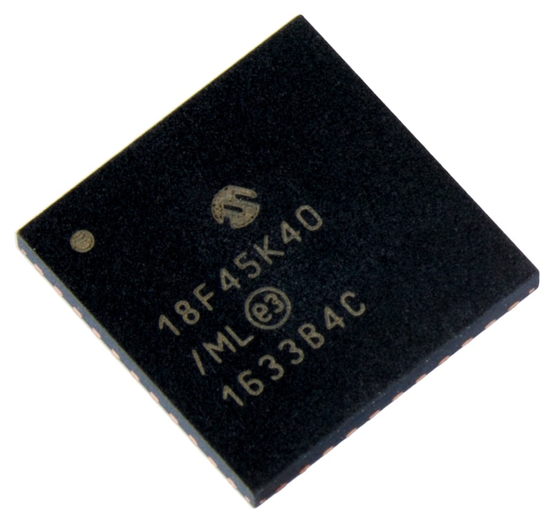
ataque Microchip PIC18F45K40T controlador de memoria es un proceso para desbloquear microcontrolador pic18f45k40t bit fusible de seguridad, y luego leer el software de memoria flash del microprocesador pic18f45k40t chipset
The first five events will cause a device Reset. The last one event is considered a continuation of program execution. To determine whether a device Reset or wake-up event occurred, refer to “Determining the Cause of a Reset” when recover microchip pic18f24k22 locked flash memory code.
When the SLEEP instruction is being executed, the next instruction (PC + 2) is prefetched. For the device to wake-up through an interrupt event, the corresponding Interrupt Enable bit must be enabled, as well as the Peripheral Interrupt Enable bit (PEIE = 1), for every interrupt not in PIR0.
Wake-up will occur regardless of the state of the GIE bit. If the GIE bit is disabled, the device continues execution at the instruction after the SLEEP instruction. If the GIE bit is enabled by restoring microcontroller pic18f25k22 memory heximal file, the device executes the instruction after the SLEEP instruction, the device will then call the Interrupt Service Routine.
In cases where the execution of the instruction following SLEEP is not desirable, the user should have a NOP after the SLEEP instruction.
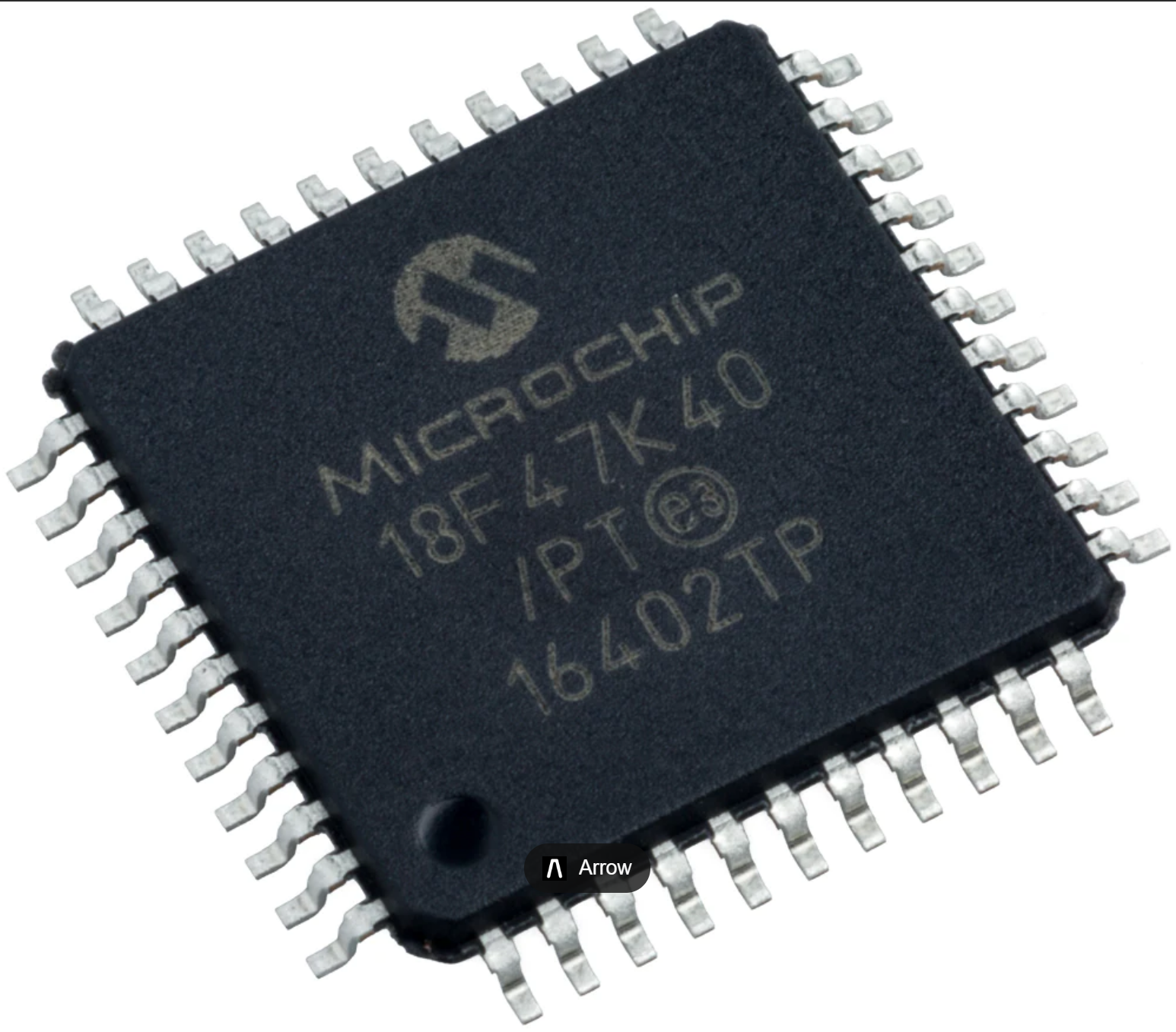
Break Microchip PIC18F47K40T Controller Flash Content
Break Microchip PIC18F47K40T Controller Flash Content needs to hack tamper resistance system of PIC18F47K40T mcu flash memory, and then extract code from pic18f47k40t microprocessor, in the format of binary or heximal;
The IOFS bit when the internal oscillator block has stabilized and is providing the system clock in RC Clock modes or during Two-Speed Start-ups. The T1RUN bit (T1CON<6>) indicates when the Timer1 oscillator is providing the system clock in Secondary Clock modes.
In power managed modes, only one of these three bits will be set at any time. If none of these bits are set, the INTRC is providing the system clock, or the internal oscillator block has just started and is not yet stable when replicate pic18f46k20 microprocessor flash program. The IDLEN bit controls the selective shutdown of the controller’s CPU in power managed modes.
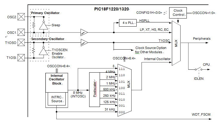
1: The Timer1 oscillator must be enabled to select the secondary clock source. The Timer1 oscillator is enabled by setting the T1OSCEN bit in the Timer1 Control reg- ister (T1CON<3>) to break pic18f46k22 mcu flash heximal memory. If the Timer1 oscillator is not enabled, then any attempt to select a secondary clock source when executing a SLEEP instruction will be ignored.
romper Microchip PIC18F47K40T controlador de contenido flash necesita para hackear sistema de resistencia a la manipulación de PIC18F47K40T mcu memoria flash, y luego extraer el código de pic18f47k40t microprocesador, en el formato de binario o heximal
2: It is recommended that the Timer1 oscil- lator be operating and stable before exe- cuting the SLEEP instruction or a very long delay may occur while the Timer1 oscillator starts.
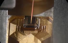
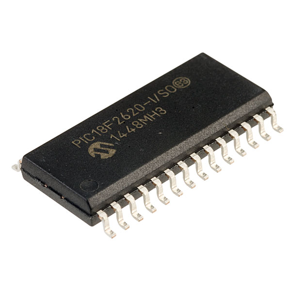
Attack Locked Microprocessor PIC18F2620T Tamper Resistance System
Attack Locked Microprocessor PIC18F2620T Tamper Resistance System and retrieve embedded firmware from microcontroller pic18f2620t flash and eeprom memory, copy encrypted content to new pic18f2620t mcu;
The OSCCON register (Register 2-2) controls several aspects of the system clock’s operation, both in full- power operation and in power managed modes.
The System Clock Select bits, SCS1:SCS0, select the clock source that is used when the device is operating in power managed modes. The available clock sources are the primary clock (defined in Configuration Register 1H) to restore flash memory content from pic18f1220t microprocessor, the secondary clock (Timer1 oscillator) and the internal oscillator block.
The clock selection has no effect until a SLEEP instruction is executed and the device enters a power managed mode of operation. The SCS bits are cleared on all forms of Reset.
The Internal Oscillator Select bits, IRCF2:IRCF0, select the frequency output of the internal oscillator block that is used to drive the system clock. The choices are the INTRC source, the INTOSC source (8 MHz), or one of the six frequencies derived from the INTOSC posts- caler (125 kHz to 4 MHz).
ataque bloqueado microprocesador PIC18F2620T sistema de resistencia a la manipulación y recuperar firmware incrustado del microcontrolador pic18f2620t flash y memoria eeprom, copiar contenido cifrado al nuevo MCU pic18f2620t
If the internal oscillator block is supplying the system clock, changing the states of these bits will have an immediate change on the inter- nal oscillator’s output by decrypting pic18f1230 microcontroller flash memory firmware. The OSTS, IOFS and T1RUN bits indicate which clock source is currently providing the system clock.
The OSTS indicates that the Oscillator Start-up Timer has timed out and the primary clock is providing the system clock in Primary Clock modes. The IOFS bit indicates
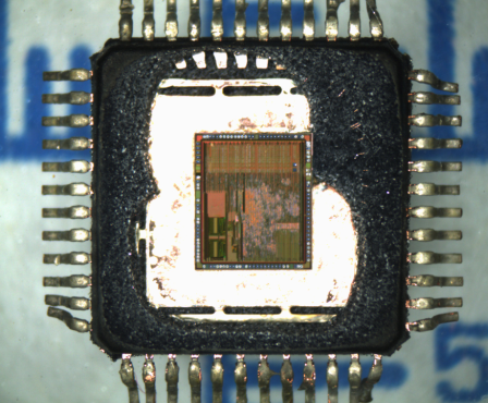
Microchip PIC18F8520 MCU Protection Breaking
The final purpose of Microchip PIC18F8520 MCU Protection Breaking is to extract embedded program from microcontroller pic18f8520, the process of dumping flash heximal and eeprom binary from microprocessor pic18f8520 will be aggressive…
PIC18F8520 devices offer only the Timer1 oscillator as a secondary oscillator. This oscillator, in all power managed modes, is often the time base for functions such as a real-time clock when decoding microcontroller pic18f1220 program from its flash memory.
Most often, a 32.768 kHz watch crystal is connected between the RB6/T1OSO and RB7/T1OSI pins. Like the LP mode oscillator circuit, loading capacitors are also connected from each pin to ground. These pins are also used during ICSP operations.
The Timer1 oscillator is discussed in greater detail in
Section 12.2 “Timer1 Oscillator”.
In addition to being a primary clock source, the internal oscillator block is available as a power managed mode clock source to decap pic18f1320 microchip processor memory. The INTRC source is also used as the clock source for several special features, such as the WDT and Fail-Safe Clock Monitor.
el propósito final de la ruptura de la protección del MCU PIC18F8520 del microchip es extraer el programa incrustado del microcontrolador pic18f8520, el proceso de volcado de flash heximal y eeprom binario del microprocesador pic18f8520 será agresivo
The clock sources for the PIC18F1220/1320 devices are shown in Figure 2-8. See Section 12.0 “Timer1 Module” for further details of the Timer1 oscillator. See Section 19.1 “Configuration Bits” for Configuration register details.
Secured Microcontroller PIC18F4610 Flash Heximal Restoring
Secured Microcontroller PIC18F4610 Flash Heximal Restoring needs to crack mcu pic18f4610 security fuse bit, and then extract embedded firmware from pic18f4610 processor flash memory;
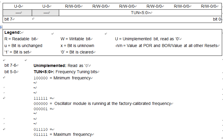
When the OSCTUNE register is modified, the INTOSC and INTRC frequencies will begin shifting to the new frequency. The INTRC clock will reach the new frequency within 8 clock cycles (approximately 8* 32 ms = 256 ms).
The INTOSC clock will stabilize within 1 ms. Code execution continues during this shift. There is no indication that the shift has occurred. Operation of features that depend on the INTRC clock source frequency, such as the WDT, Fail-Safe Clock Monitor and peripherals, will also be affected by the change in frequency.
Like previous PIC18 devices, the PIC18F4610 devices include a feature that allows the system clock source to be switched from the main oscillator to an alternate low-frequency clock source when crack pic18f4550 microcontroller flash memory. PIC18F4610 devices offer two alternate clock sources. When enabled, these give additional options for switching to the various power managed operating modes.
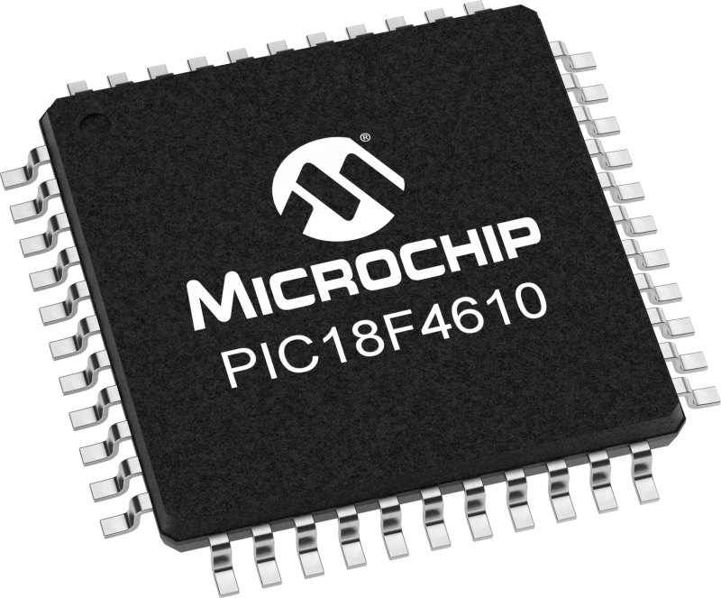
microcontrolador seguro PIC18F4610 flash heximal restauración necesita descifrar MCU pic18f4610 bit de fusible de seguridad, y luego extraer firmware incrustado de la memoria flash del procesador pic18f4610
Essentially, there are three clock sources for these devices:
- Primary oscillators
- Secondary oscillators
- Internal oscillator block
The primary oscillators include the External Crystal and Resonator modes, the External RC modes, the External Clock modes and the internal oscillator block in the process of copying binary file from pic18f458 mcu. The particular mode is defined on POR by the contents of Configuration Register 1H.
The details of these modes are covered earlier in this chapter. The secondary oscillators are those external sources not connected to the OSC1 or OSC2 pins. These sources may continue to operate even after the controller is placed in a power managed mode.