Archive for the ‘Break IC’ Category
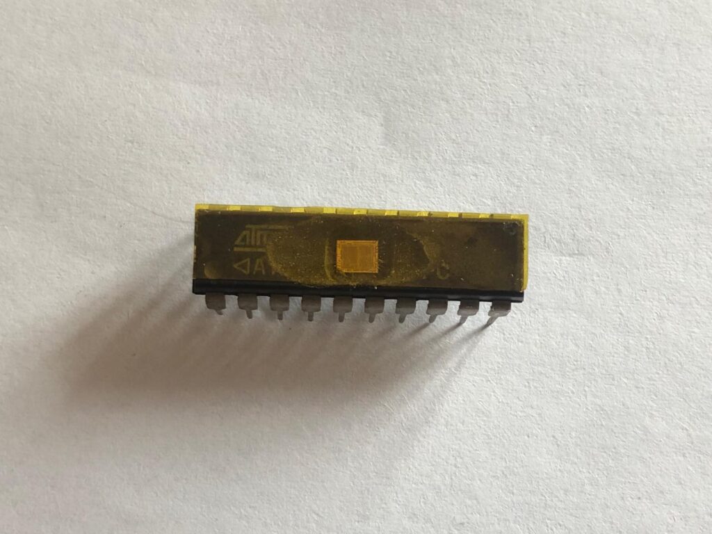
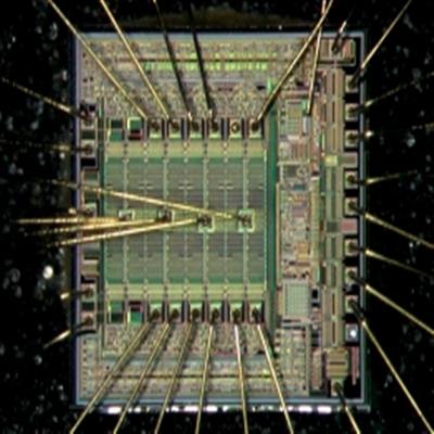
 Attack Texas Instrument MSP430G2544 CPU Flash Memory
Attack Texas Instrument MSP430G2544 CPU Flash Memory can help engineer to extract embedded firmware from microcontroller msp430g2544 flash memory and then duplicate the binary to new MCU msp430g2544;
Typical applications include sensor systems that capture analog signals, convert them to digital values, and then process the data for display or for transmission to a host system. Stand-alone radio-frequency (RF) sensor front ends are another area of application.
Stresses beyond those listed under Absolute Maximum Ratings may cause permanent damage to the device. These are stress ratings only, and functional operation of the device at these or any other conditions beyond those indicated under Recommended Operating Conditions is not implied to carry out the attacking over mcu msp430g2312 protective flash memory code ,Exposure to absolute-maximum-rated conditions for extended periods may affect device reliability.
атака флеш-пам’яті Texas Instrument MSP430G2544 CPU може допомогти інженеру витягти вбудовану прошивку з флеш-пам’яті мікроконтролера msp430g2544, а потім скопіювати двійковий файл на новий MCU msp430g2544
All voltages referenced to VSS.
The JTAG fuse-blow voltage, VFB, is allowed to exceed the absolute maximum rating. The voltage is applied to the TEST pin when blowing the JTAG fuse.
saldırı Texas Instrument MSP430G2544 CPU flash bellek, mühendisin mikrodenetleyici msp430g2544 flash bellekten gömülü bellenimi çıkarmasına ve ardından ikili dosyayı yeni MCU msp430g2544’e çoğaltmasına yardımcı olabilir
Higher temperature may be applied during board soldering process according to the current JEDEC J-STD-020 specification with peak reflow temperatures not higher than classified on the device label on the shipping boxes or reels.
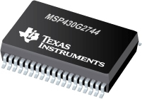
Break Mixed Signal MSP430G2744 Flash Memory
Break Mixed Signal MSP430G2744 Flash Memory and write the flash memory program to new msp430g2744 microcontroller for cloning;
The Texas Instruments MSP430™ family of ultra-low-power microcontrollers consists of several devices featuring different sets of peripherals targeted for various applications. The architecture, combined with five low-power modes, is optimized to achieve extended battery life in portable measurement applications.
розбити змішаний сигнал MSP430G2744 флеш-пам’ять і записати програму флеш-пам’яті на новий мікроконтролер MSP430G2744 для клонування;
The device features a powerful 16-bit RISC CPU, 16-bit registers, and constant generators that contribute to maximum code efficiency. The digitally controlled oscillator (DCO) allows the device to wake up from low-power modes to active mode in less than 1 µs.
Flash bellek MSP430G2744 karışık sinyali kırın ve klonlama için yeni MSP430G2744 mikrodenetleyiciye flash bellek programını yazın;
The MSP430G2x44 series is an ultra-low-power mixed-signal microcontroller with two built-in 16-bit timers, a universal serial communication interface (USCI), 10-bit analog-to-digital converter (ADC) with integrated reference and data transfer controller (DTC), and 32 I/O pins which are critical features for locked microcontroller msp430g2452 flash memory breaking.
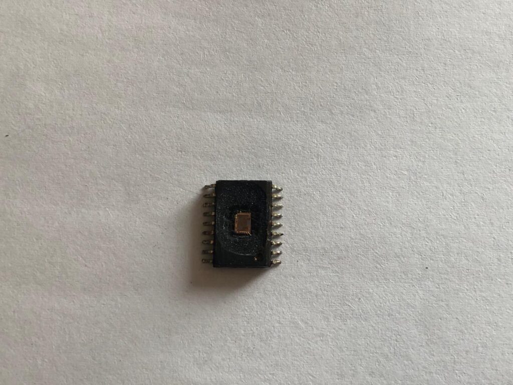
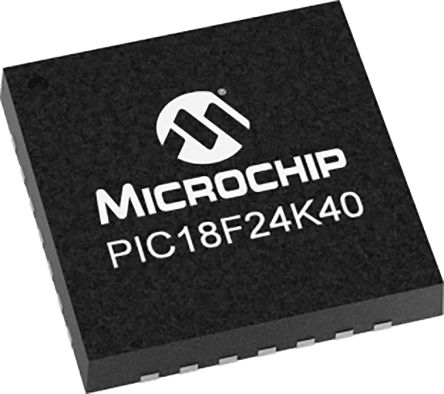
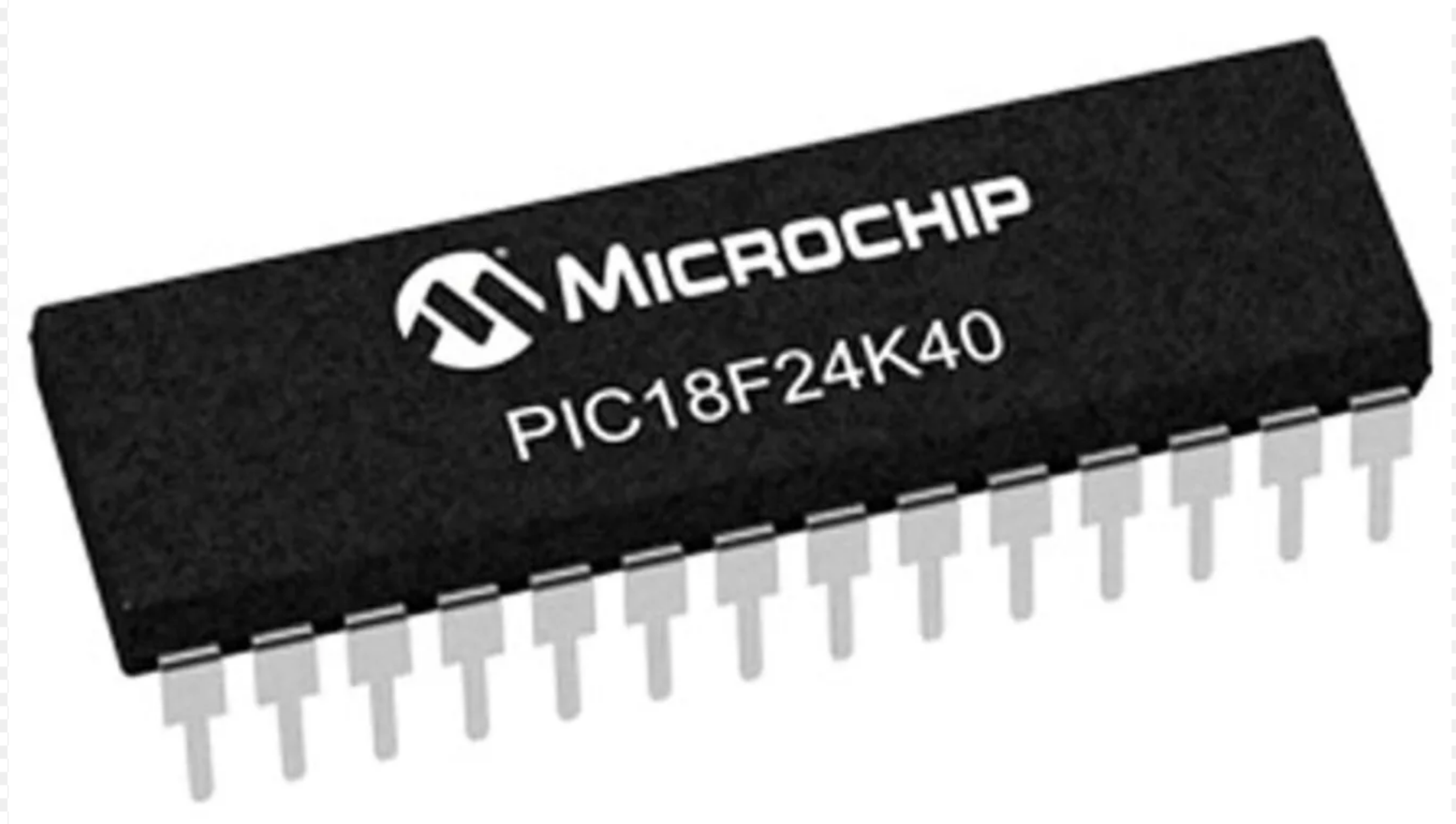
Break Microchip PIC18F24K40 Controller Protective Flash Memory
Break Microchip PIC18F24K40 Controller Protective Flash Memory and readout embedded firmware from Microcontroller, the locked source code will be restored from mcu pic18f24k40;
Break Microchip PIC18F24K40 Controller Protective Flash Memory and readout embedded firmware from Microcontroller, the locked source code will be restored from mcu pic18f24k40;
The HFINTOSC/MFINTOSC oscillator circuits are factory calibrated but can be adjusted in software by writing to the TUN<5:0> bits of the OSCTUNE register (Register 2-3). The default value of the TUN<5:0> is ‘000000’. The value is a 6-bit two’s complement number.
When the OSCTUNE register is modified, the HFINTOSC/MFINTOSC frequency will begin shifting to the new frequency. Code execution continues during this shift. There is no indication that the shift has occurred. The TUN<5:0> bits in OSCTUNE do not affect the LFINTOSC frequency. Operation of features that depend on the LFINTOSC clock source frequency, such as the Power-up Timer (PWRT), Watchdog Timer (WDT), Fail-Safe Clock Monitor (FSCM) and peripherals, are not affected by the change in frequency.
mikroçip PIC18F24K40 denetleyici koruyucu flash belleğini kırın ve mikrodenetleyiciden gömülü bellenimi okuyun, kilitli kaynak kodu MCU PIC18F24K40’tan geri yüklenecektir;
The OSCTUNE register also implements the INTSRC and PLLEN bits, which control certain features of the internal oscillator block. The INTSRC bit allows users to select which internal oscillator provides the clock source when the 31.25 kHz frequency option is selected. This is covered in greater detail in Section 2.2.3 “Low Frequency Selection”. The PLLEN bit controls the operation of the frequency multiplier, PLL, in internal oscillator modes. For more details about the function of the PLLEN bit, see Section 2.6.2 “PLL in HFINTOSC Modes”
Quebre a memória flash protetora do controlador de PIC18F24K40 do microchip e leia o firmware incorporado do microcontrolador, o código-fonte bloqueado será restaurado a partir do MCU PIC18F24K40;
The Low-Frequency Internal Oscillator (LFINTOSC) is a 31.25 kHz internal clock source. The LFINTOSC is not tunable, but is designed to be stable across temperature and voltage. See Section 27.0 “Electrical Char- acteristics” for the LFINTOSC accuracy specifications. The output of the LFINTOSC can be a clock source to the primary clock or the INTOSC clock (see Figure 2-1). The LFINTOSC is also the clock source for the Power- up Timer (PWRT), Watchdog Timer (WDT) and Fail-Safe Clock Monitor (FSCM).
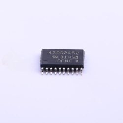
Locked Microcontroller MSP430G2452 Flash Memory Breaking
Locked Microcontroller MSP430G2452 Flash Memory Breaking is a process to crack secured msp430g2452 protective fuse bit by focus ion beam and then extract flash memory program from mcu msp430g2452;
FEATURES of MSP430G2402 can help us find a proper way to Decipher Texas Instruments MCU MSP430G2402:
Low Supply Voltage Range: 1.8 V to 3.6 V
Ultra-Low Power Consumption
– Active Mode: 220 µA at 1 MHz, 2.2 V
– Standby Mode: 0.5 µA
– Off Mode (RAM Retention): 0.1 µA
Ultra-Fast Wake-Up From Standby Mode in
Less Than 1 µs
Kilitli mikrodenetleyici MSP430G2452 flash bellek kırma, güvenli MSP430G2452 koruyucu sigortayı odak iyon ışını ile bit kırmak ve daha sonra MCU MSP430G2452’den flash bellek programını çıkarmak için yapılan bir işlemdir
16-Bit RISC Architecture, 62.5-ns Instruction Cycle Time
Basic Clock Module Configurations
– Internal Frequencies up to 16 MHz With
Four Calibrated Frequencies
– Internal Very-Low-Power Low-Frequency
(LF) Oscillator
– 32-kHz Crystal
– External Digital Clock Source
One 16-Bit Timer_A With Three
Capture/Compare Registers
Up to 16 Touch-Sense Enabled I/O
Universal Serial Interface (USI) Supporting SPI and I2C
10-Bit 200-ksps Analog-to-Digital (A/D)
Converter With Internal Reference,
Sample-and-Hold, and Autoscan
(MSP430G2x32 Only)
Brownout Detector
Serial Onboard Programming,
No External Programming Voltage Needed,
Programmable Code Protection by Security Fuse which can be removed by break msp430g2412 flash memory
On-Chip Emulation Logic With Spy-Bi-Wire Interface
Family Members are Summarized in Table 1
Заблокований мікроконтролер MSP430G2452 розрив флеш-пам’яті – це процес злому захищеного захисного запобіжника MSP430G2452 бітом за допомогою фокусування іонного променя, а потім вилучення програми флеш-пам’яті з MCU MSP430G2452
Package Options
– TSSOP: 14 Pin, 20 Pin
– PDIP: 20 Pin
– QFN: 16 Pin
For Complete Module Descriptions, See the
MSP430x2xx Family User’s Guide (SLAU144)
Break Texas Instrument MSP430G2412 Locked Flash Memory
Break Texas Instrument MSP430G2412 Locked Flash Memory and extract flash memory heximal program from msp430g2412, the security fuse bit will be compromised and replicate flash memory heximal to new msp430g2412 MCU;
The clock system is supported by the basic clock module that includes support for a 32768-Hz watch crystal oscillator, an internal very-low-power low-frequency oscillator and an internal digitally controlled oscillator (DCO).
The basic clock module is designed to meet the requirements of both low system cost and low power consumption which can be used for breaking msp430g2312 protected flash memory. The internal DCO provides a fast turn-on clock source and stabilizes in less than 1 µs. The basic clock module provides the following clock signals:
casser Texas Instrument MSP430G2412 la mémoire flash verrouillée et extraire le programme heximal de mémoire flash de msp430g2412, le bit de fusible de sécurité sera compromis et répliquera la mémoire flash hexamale sur le nouveau microcontrôleur msp430g2412;
- Auxiliary clock (ACLK), sourced either from a 32768-Hz watch crystal or the internal LF oscillator.
- Main clock (MCLK), the system clock used by the CPU.
- Sub-Main clock (SMCLK), the sub-system clock used by the peripheral modules.
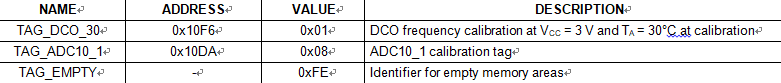
The DCO settings to calibrate the DCO output frequency are stored in the information memory segment A.
Calibration Data Stored in Information Memory Segment A
σπάστε το όργανο του Τέξας MSP430G2412 κλειδωμένη μνήμη flash και εξαγάγετε το δεκαεξαδικό πρόγραμμα μνήμης flash από το msp430g2412, το κομμάτι ασφάλειας ασφάλειας θα παραβιαστεί και θα αναπαράγει τη μνήμη flash δεκαεξαδική στο νέο msp430g2412 MCU.
Calibration data is stored for both the DCO and for ADC10 organized in a tag-length-value structure.
Attack MSP430G2312 Microcontroller Protected Flash Memory
Attack MSP430G2312 Microcontroller Protected Flash Memory and make flash memory program cloned file from mcu 430g2312, extract ti processor’s locked code from msp430g2312 flash memory;
The flash memory can be programmed via the Spy-Bi-Wire/JTAG port or in-system by the CPU. The CPU can perform single-byte and single-word writes to the flash memory. Features of the flash memory include:
- Flash memory has n segments of main memory and four segments of information memory (A to D) of 64 bytes each. Each segment in main memory is 512 bytes in size.
- Segments 0 to n may be erased in one step, or each segment may be individually erased.
- Segments A to D can be erased individually or as a group with segments 0 to n. Segments A to D are also called information memory.
- Segment A contains calibration data. After reset, segment A is protected against programming and erasing. It can be unlocked, but care should be taken not to erase this segment if the device-specific calibration data is required.
Peripherals are connected to the CPU through data, address, and control buses and can be handled using all instructions when restoring ti mcu 430g2101 flash content. For complete module descriptions, see the MSP430x2xx Family User‘s Guide (SLAU144).
Mixed Signal Microcontroller MSP430G2212 Flash Program Reverse Reading
Mixed Signal Microcontroller MSP430G2212 Flash Program Reverse Reading starts from cracking texas instrument msp430g2212 fuse bit, and readout embedded firmware from MSP430G2212 flash memory;
The MSP430 CPU has a 16-bit RISC architecture that is highly transparent to the application. All operations, other than program-flow instructions, are performed as register operations in conjunction with seven addressing modes for source operand and four addressing modes for destination operand.
The CPU is integrated with 16 registers that provide reduced instruction execution time. The register-to-register operation execution time is one cycle of the CPU clock when breaking texas instrument msp430g2352 microprocessor protection.
Four of the registers, R0 to R3, are dedicated as program counter, stack pointer, status register, and constant generator, respectively. The remaining registers are general-purpose registers.
Peripherals are connected to the CPU using data, address, and control buses, and can be handled with all instructions. The instruction set consists of the original 51 instructions with three formats and seven address modes and additional instructions for the expanded address range. Each instruction can operate on word and byte data.
Reverse Texas Instrument MSP430G2112 Microcontroller Flash Memory
Reverse Texas Instrument MSP430G2112 Microcontroller Flash Memory is a process to unlock secured msp430g2112 mcu flash memory and then extract firmware program from msp430g2112 processor;
The Texas Instruments MSP430™ family of ultra-low-power microcontrollers consist of several devices featuring different sets of peripherals targeted for various applications. The architecture, combined with five low-power modes, is optimized to achieve extended battery life in portable measurement applications.
The device features a powerful 16-bit RISC CPU, 16-bit registers, and constant generators that contribute to maximum code efficiency. The digitally controlled oscillator (DCO) allows wake-up from low-power modes to active mode in less than 1 µs.
The MSP430G2x52 and MSP430G2x12 series of microcontrollers are ultra-low-power mixed signal microcontrollers with built-in 16-bit timers, and up to 16 I/O touch sense enabled pins and built-in communication capability using the universal serial communication interface and have a versatile analog comparator when restoring mixed signal mcu flash binary code.
The MSP430G2x52 series have a 10-bit A/D converter. For configuration details. Typical applications include low-cost sensor systems that capture analog signals, convert them to digital values, and then process the data for display or for transmission to a host system.
Break Mixed Signal MSP430G2211 Microcontroller Flash Memory
Break Mixed Signal MSP430G2211 Microcontroller Flash Memory and duplicate the embedded firmware from MSP430G2211 mcu memory in the format of heximal, copy firmware to new Microprocessor to perform the same functions:
Timer_A2 is a 16-bit timer/counter with two capture/compare registers. Timer_A2 can support multiple capture/compares, PWM outputs, and interval timing.
Timer_A2 also has extensive interrupt capabilities. Interrupts may be generated from the counter on overflow conditions and from each of the capture/compare registers.
The primary function of the comparator_A+module is to support precision slope analog-to-digital conversions, battery-voltage supervision, and monitoring of external analog signals which can be used for restoring microcontroller msp430g2101 flash content.
- Stresses beyond those listed under “absolute maximum ratings” may cause permanent damage to the device. These are stress ratings only, and functional operation of the device at these or any other conditions beyond those indicated under “recommended operating conditions” is not implied. Exposure to absolute-maximum-rated conditions for extended periods may affect device reliability.
- All voltages referenced to VSS. The JTAG fuse-blow voltage, VFB, is allowed to exceed the absolute maximum rating. The voltage is applied to the TEST pin when blowing the JTAG fuse.
- Higher temperature may be applied during board soldering according to the current JEDEC J-STD-020 specification with peak reflow temperatures not higher than classified on the device label on the shipping boxes or reels.
Attack Texas Instrument MSP430G2111 Microprocessor
Attack Texas Instrument MSP430G2111 Microprocessor and clone mcu msp430g2111 flash memory program from original MCU, copy binary firmware to new microcontroller;
The flash memory can be programmed via the Spy-Bi-Wire/JTAG port or in-system by the CPU. The CPU can perform single-byte and single-word writes to the flash memory. Features of the flash memory include:
- Flash memory has n segments of main memory and four segments of information memory (A to D) of 64 bytes each. Each segment in main memory is 512 bytes in size.
- Segments 0 to n may be erased in one step, or each segment may be individually erased.
- Segments A to D can be erased individually or as a group with segments 0 to n. Segments A to D are also called information memory.
- Segment A contains calibration data. After reset segment A is protected against programming and erasing. It can be unlocked but care should be taken not to erase this segment if the device-specific calibration data is required.