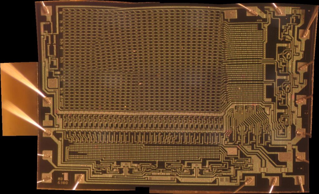
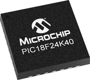
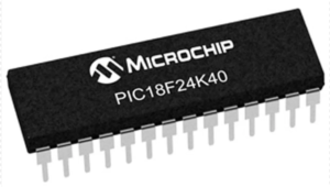
 Break Microchip PIC18F24K40 Controller Protective Flash Memory
Break Microchip PIC18F24K40 Controller Protective Flash Memory and readout embedded firmware from Microcontroller, the locked source code will be restored from mcu pic18f24k40;

Break Microchip PIC18F24K40 Controller Protective Flash Memory and readout embedded firmware from Microcontroller, the locked source code will be restored from mcu pic18f24k40;
The HFINTOSC/MFINTOSC oscillator circuits are factory calibrated but can be adjusted in software by writing to the TUN<5:0> bits of the OSCTUNE register (Register 2-3). The default value of the TUN<5:0> is ‘000000’. The value is a 6-bit two’s complement number.
When the OSCTUNE register is modified, the HFINTOSC/MFINTOSC frequency will begin shifting to the new frequency. Code execution continues during this shift. There is no indication that the shift has occurred. The TUN<5:0> bits in OSCTUNE do not affect the LFINTOSC frequency. Operation of features that depend on the LFINTOSC clock source frequency, such as the Power-up Timer (PWRT), Watchdog Timer (WDT), Fail-Safe Clock Monitor (FSCM) and peripherals, are not affected by the change in frequency.

mikroçip PIC18F24K40 denetleyici koruyucu flash belleğini kırın ve mikrodenetleyiciden gömülü bellenimi okuyun, kilitli kaynak kodu MCU PIC18F24K40’tan geri yüklenecektir;
The OSCTUNE register also implements the INTSRC and PLLEN bits, which control certain features of the internal oscillator block. The INTSRC bit allows users to select which internal oscillator provides the clock source when the 31.25 kHz frequency option is selected. This is covered in greater detail in Section 2.2.3 “Low Frequency Selection”. The PLLEN bit controls the operation of the frequency multiplier, PLL, in internal oscillator modes. For more details about the function of the PLLEN bit, see Section 2.6.2 “PLL in HFINTOSC Modes”

Quebre a memória flash protetora do controlador de PIC18F24K40 do microchip e leia o firmware incorporado do microcontrolador, o código-fonte bloqueado será restaurado a partir do MCU PIC18F24K40;
The Low-Frequency Internal Oscillator (LFINTOSC) is a 31.25 kHz internal clock source. The LFINTOSC is not tunable, but is designed to be stable across temperature and voltage. See Section 27.0 “Electrical Char- acteristics” for the LFINTOSC accuracy specifications. The output of the LFINTOSC can be a clock source to the primary clock or the INTOSC clock (see Figure 2-1). The LFINTOSC is also the clock source for the Power- up Timer (PWRT), Watchdog Timer (WDT) and Fail-Safe Clock Monitor (FSCM).