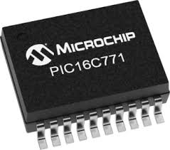
 Break IC PIC16C771 Firmware
The Special Function Registers are registers used by the CPU and Peripheral Modules for controlling the desired operation of the device to facilitate the process of Break IC PIC16C771 Firmware. These registers are implemented as static RAM, core (CPU) and peripheral. Those registers associated with the core functions are described in detail in this section. Those related to the operation of the peripheral features are described in detail in that peripheral feature section. For example, CLRF STATUS will clear the upper-three;
The STATUS register, shown in Register 2-1, contains the arithmetic status of the ALU, the RESET status and the bank select bits for data memory.
The STATUS register can be the destination for any instruction, as with any other register. If the STATUS register is the destination for an instruction that affects the Z, DC or C bits, then the write to these three bits is disabled.
These bits are set or cleared according to the device logic. Furthermore, the TO and PD bits are not writable. Therefore, the result of an instruction with the STATUS register as destination may be different than intended.
It is recommended, therefore, that only BCF, BSF, SWAPF and MOVWF instructions are used to alter the STATUS register, because these instructions do not affect the Z, C or DC bits from the STATUS register. For other instructions not affecting any status bits, see the ”Instruction Set Summary.
The program counter (PC) specifies the address of the instruction to fetch for execution. The PC is 13 bits wide. The low byte is called the PCL register. This register is readable and writable in order to Break IC PIC16C771 Firmware. The high byte is called the PCH register. This register contains the PC<12:8> bits and is not directly readable or writable. All updates to the PCH register occur through the PCLATH register.
PIC16C717/770/771 devices are capable of addressing a continuous 8K word block of program memory. The CALL and GOTO instructions provide only 11 bits of address to allow branching within any 2K program memory page. When doing aCALL or GOTO instruction, the upper 2 bits of the address are provided by PCLATH<4:3>. When doing a CALL or GOTO instruction, the user must ensure that the page select bits are programmed so that the desired program memory page is addressed.
A return instruction pops a PC address off the stack onto the PC register. Therefore, manipulation of the PCLATH<4:3> bits are not required for the return instructions (which POPs the address from the stack).

Break IC PIC16C771 Firmware
The stack allows a combination of up to 8 program calls and interrupts to occur. The stack contains the return address from this branch in program execution. Mid-range devices have an 8-level deep x 13-bit wide hardware stack. The stack space is not part of either program or data space and the stack pointer is not readable or writable which is not easy for Recover Chip PIC16F689 Flash. The PC is PUSHed onto the stack when a CALL instruction is executed or an interrupt causes a branch. The stack is POPed in the event of RETURN, RETLW or a RETFIE instruction execution. PCLATH is not modified when the stack is PUSHed or POPed.
After the stack has been PUSHed eight times, the ninth push overwrites the value that was stored from the first push. The tenth push overwrites the second push (and so on).
The INDF register is not a physical register. Addressing INDF actually addresses the register whose address is contained in the FSR register (FSR is a pointer). This is indirect addressing before Microcontroller Unlock.
Reading INDF itself indirectly (FSR = 0) will produce 00h. Writing to the INDF register indirectly results in a no-operation (although STATUS bits may be affected). A simple program to clear RAM locations 20h-2Fh using indirect addressing is shown in Example 2-1 Some pins for these I/O ports are multiplexed with an alternate function for the peripheral features on the device by PIC16F84A Microcontroller Chip Attack. In general, when a peripheral is enabled, that pin may not be used as a general purpose I/O pin.
Additional information on I/O ports may be found in the PICmicro™ Mid-Range Reference Manual, (DS33023).
PORTA is a 8-bit wide bi-directional port. The corre-analog mode of the corresponding pins. sponding data direction register is TRISA. Setting a TRISA bit (=1) will make the corresponding PORTA pin an input, i.e., put the corresponding output driver in a hi-impedance mode. Clearing a TRISA bit (=0) will make the corresponding PORTA pin an output, i.e., put the contents of the output latch on the selected pin.