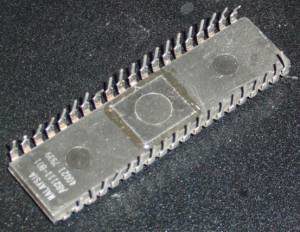
 Break IC PIC12F639 Heximal
Break IC PIC12F639 Heximal
Break IC PIC12F639 Heximal from its memory needs to know its memory organization
PROGRAM MEMORY ORGANIZATION
The PIC16F639 devices have a 13-bit program counter capable of addressing an 8K x 14 program memory space. Only the first 1K x 14 (0000h-03FFh, for the PIC12F635) and 2K x 14 (0000h-07FFh, for the PIC16F636/639) is physically implemented. Accessing a location above these boundaries will cause a wrap around within the first 2K x 14 space. The Reset vector is at 0000h and the interrupt vector is at 0004h.
DATA MEMORY ORGANIZATION
The data memory (see below Figure) is partitioned into two banks, which contain the General Purpose Registers (GPR) and the Special Function Registers (SFR).
The Special Function Registers are located in the first 32 locations of each bank. Register locations 20h-7Fh in Bank 0 and A0h-BFh in Bank 1 are GPRs, implemented as static RAM for the PIC16F639.For the PIC12F635, register locations 40h through 7Fh are GPRs implemented as static RAM. Register locations F0h-FFh in Bank 1 point to addresses 70h-7Fh in Bank 0. All other RAM is unimplemented and returns ‘0’ when read. RP0 (STATUS<5>) is the bank select bit.
GENERAL PURPOSE REGISTER
The register file is organized as 64 x 8 for the PIC12F635 and 128 x 8 for the PIC16F636/639. Each register is accessed, either directly or indirectly, through the File Select Register;
SPECIAL FUNCTION REGISTERS
The Special Function Registers (SFRs) are registers used by the CPU and peripheral functions for controlling the desired operation of the device. These registers are static RAM. The special registers can be classified into two sets: core and peripheral. The Special Function Registers associated with the “core” are described in this section. Those related to the operation of the peripheral features are described in the section of that peripheral feature from MCU CRACK.
