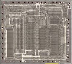
 Break IC ATmega32A Software
Breaking IC ATmega32A software involves cracking or decoding the secured and encrypted firmware stored in the microcontroller’s flash memory and EEPROM memory. The ATmega32A MCU, like many modern microprocessors, is designed with protective measures to prevent unauthorized access to its program, binary, and source code. To unlock and restore this software, reverse engineering techniques are often employed.
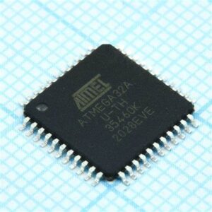
breaking IC ATmega32A software involves cracking or decoding the secured and encrypted firmware stored in the ATmega32A microcontroller’s flash memory and EEPROM memory. The ATmega32A MCU, like many modern microprocessors, is designed with protective measures to prevent unauthorized access to its program, binary, and source code. To unlock and restore this software, reverse engineering techniques are often employed
The first step in breaking the IC’s software is to analyze the microprocessor’s architecture and security features. These security mechanisms, which may include encryption or lockouts, are intended to protect the integrity of the firmware. Once these protective layers are bypassed, the embedded program can be extracted from the flash memory and EEPROM memory. The extracted binary or heximal data is then decoded to retrieve the source code, which can be restored, cloned, or replicated for use in different applications.
Unlocking the ATmega32A software also opens the door to cloning the firmware for use in other devices or systems. This process ensures that the program can be duplicated for backup purposes or hardware replication. Additionally, breaking the software can allow for troubleshooting or upgrading the system, especially when original source code or design files are unavailable.
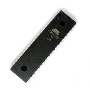
разбиване на IC Софтуерът ATmega32A включва кракване или декодиране на защитения и криптиран фърмуер, съхраняван във флаш паметта и EEPROM паметта на микроконтролера ATmega32A. ATmega32A MCU, подобно на много съвременни микропроцесори, е проектиран със защитни мерки за предотвратяване на неоторизиран достъп до неговата програма, двоичен и изходен код. За отключване и възстановяване на този софтуер често се използват техники за обратно инженерство
While breaking IC ATmega32A software can be a valuable technique for system recovery or hardware maintenance, it is essential to operate within legal and ethical boundaries. Unauthorized cracking, decoding, or cloning of software can violate intellectual property rights and lead to legal consequences. Proper authorization and adherence to intellectual property laws are essential when performing these activities.
We can Break IC ATMEGA32A Software, please view the IC ATMEGA32A features for your reference:
In order to maximize performance and parallelism, the AVR uses a Harvard architecture – with separate memories and buses for program and data. Instructions in the program memory are executed with a single level pipelining. While one instruction is being executed, the next instruction is pre-fetched from the program memory. This concept enables instructions to be executed in every clock cycle. The program memory is In-System Reprogrammable Flash memory. The fast-access Register File contains 32 x 8-bit general purpose working registers with a single clock cycle access time. This allows single-cycle Arithmetic Logic Unit (ALU) operation. In a typical ALU operation, two operands are output from the Register File, the operation is executed, and the result is stored back in the Register File – in one clock cycle. Six of the 32 registers can be used as three 16-bit indirect address register pointers for Data Space addressing – enabling efficient address calculations before Break IC.
One of the these address pointers can also be used as an address pointer for look up tables in Flash Program memory. These added function registers are the 16-bit X-, Y-, and Z-register, described later in this section. The ALU supports arithmetic and logic operations between registers or between a constant and a register. Single register operations can also be executed in the ALU. After an arithmetic operation, the Status Register is updated to reflect information about the result of the operation. Program flow is provided by conditional and unconditional jump and call instructions, able to directly address the whole address space. Most AVR instructions have a single 16-bit word format when Break IC.
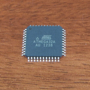
IC ATmega32A yazılımını kırmak, ATmega32A mikrodenetleyicisinin flaş belleğinde ve EEPROM belleğinde saklanan güvenli ve şifreli aygıt yazılımını kırmayı veya kodunu çözmeyi içerir. ATmega32A MCU, birçok modern mikroişlemci gibi, programına, ikili dosyasına ve kaynak koduna yetkisiz erişimi önlemek için koruyucu önlemlerle tasarlanmıştır. Bu yazılımın kilidini açmak ve geri yüklemek için genellikle tersine mühendislik teknikleri kullanılır
Every program memory address contains a 16- or 32-bit instruction. Program Flash memory space is divided in two sections, the Boot program section and the Application Program section. Both sections have dedicated Lock bits for write and break/write protection. The SPM instruction that writes into the Application Flash memory section must reside in the Boot Program section. During interrupts and subroutine calls, the return address Program Counter (PC) is stored on the Stack. The Stack is effectively allocated in the general data SRAM, and consequently the Stack size is only limited by the total SRAM size and the usage of the SRAM. All user programs must initialize the SP in the reset routine (before subroutines or interrupts are executed). The Stack Pointer SP is break/write accessible in the I/O space.
The data SRAM can easily be accessed through the five different addressing modes supported in the AVR architecture. The memory spaces in the AVR architecture are all linear and regular memory maps. A flexible interrupt module has its control registers in the I/O space with an additional global interrupt enable bit in the Status Register. All interrupts have a separate interrupt vector in the interrupt vector table after Break IC.
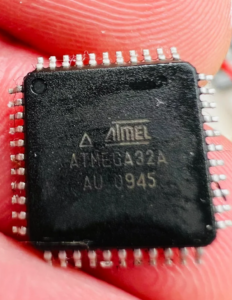
IC ATmega32A 소프트웨어를 깨는 것은 ATmega32A 마이크로컨트롤러의 플래시 메모리와 EEPROM 메모리에 저장된 보안되고 암호화된 펌웨어를 크래킹하거나 디코딩하는 것을 포함합니다. 많은 최신 마이크로프로세서와 마찬가지로 ATmega32A MCU는 프로그램, 바이너리 및 소스 코드에 대한 무단 액세스를 방지하기 위한 보호 조치로 설계되었습니다. 이 소프트웨어의 잠금을 해제하고 복원하기 위해 종종 역엔지니어링 기술이 사용됩니다.
The interrupts have priority in accordance with their interrupt vector position. The lower the interrupt vector address, the higher the priority. The I/O memory space contains 64 addresses for CPU peripheral functions as Control Registers, SPI, and other I/O functions. The I/O Memory can be accessed directly, or as the Data Space locations following those of the Register File, $20 – $5F.
