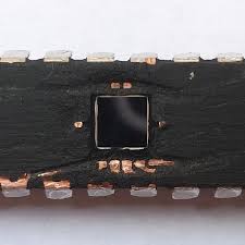
 Attack Renesas R5F51115ADFM#3A MCU Flash Memory
Attack Renesas R5F51115ADFM#3A MCU Flash Memory and extract embedded binary from microcontroller flash memory and download it to new MCU for cloning purpose;

During sleep mode or mode transitions, do not write to the system control related registers (indicated by ‘SYSTEM’ in the Module Symbol column in Table 4.1, List of I/O Registers (Address Order)).
Permanent damage to the MCU may result if absolute maximum ratings are exceeded.
To preclude any malfunctions due to noise interference, insert capacitors of high frequency characteristics between the VCC and VSS pins, between the AVCC0 and AVSS0 pins, between the VCC_USB and VSS_USB pins, and between the VREFH0 and VREFL0 pins.

атакувати флеш-пам’ять MCU Renesas R5F51115ADFM#3A і витягти вбудовану двійкову або шістнадцяткову програмну прошивку з флеш-пам’яті мікроконтролера R5F51115ADFM#3A і скопіювати її в новий MCU з метою клонування;
Place capacitors of about 0.1 μF as close as possible to every power supply pin and use the shortest and heaviest possible traces. Also, connect capacitors as stabilization capacitance which will help to facilitate the process of cracking renesas mcu r5f563nfddf flash memory.
Connect the VCL pin to a VSS pin via a 4.7 μF capacitor. The capacitor must be placed close to the pin, refer to section 5.12.1, Connecting VCL Capacitor and Bypass Capacitors.
Do not input signals or an I/O pull-up power supply to ports other than 5-V tolerant ports while the device is not powered. The current injection that results from input of such a signal or I/O pull-up may cause malfunction and the abnormal current that passes in the device at this time may cause degradation of internal elements.

Renesas R5F51115ADFM#3A MCU flash belleğe saldırın ve mikrodenetleyici R5F51115ADFM#3A flash bellekten gömülü ikili veya onaltılık program bellenimini çıkarın ve klonlama amacıyla yeni MCU’ya kopyalayın;
If input voltage (within the specified range from -0.3 to + 6.5V) is applied to 5-V tolerant ports, it will not cause problems such as damage to the MCU.