 Attack Chip dsPIC33FJ256GP506A Software
The dsPIC33FJ256GP506A is a high-performance digital signal controller from Microchip, widely used in industrial, automotive, and embedded systems. However, its security mechanisms can be compromised through advanced techniques such as firmware dumping, reverse engineering, and decryption. This article explores methods to crack, decode, and clone the program stored in its flash memory and EEPROM.
El dsPIC33FJ256GP506A es un controlador de señales digitales de alto rendimiento de Microchip, ampliamente utilizado en sistemas industriales, automotrices y embebidos. Sin embargo, sus mecanismos de seguridad pueden verse comprometidos mediante técnicas avanzadas como el volcado de firmware, la ingeniería inversa y el descifrado. Este artículo explora métodos para descifrar, decodificar y clonar el programa almacenado en su memoria flash y EEPROM.
1. Dumping Firmware from Flash Memory
The primary step in attacking the dsPIC33FJ256GP506A is extracting the binary code from its internal flash memory. Attackers often use hardware tools like a programmer/debugger (PICKit, ICD, or J-Tag) to dump the firmware. If read protection is enabled, more invasive methods like decapsulating the chip and using microprobing or laser fault injection may be required.
Once extracted, the heximal data can be analyzed using disassemblers (IDA Pro, Ghidra) to reverse engineer the source code.
2. Breaking EEPROM Memory Protection
Many devices store critical data (encryption keys, calibration values) in EEPROM memory. Attackers can dump EEPROM contents using I2C/SPI sniffers or direct memory reading via debug interfaces. If the data is encrypted, brute-force attacks or side-channel analysis may help decrypt it.
DsPIC33FJ256GP506A to wydajny cyfrowy kontroler sygnału firmy Microchip, szeroko stosowany w systemach przemysłowych, motoryzacyjnych i wbudowanych. Jednak jego mechanizmy bezpieczeństwa mogą zostać naruszone za pomocą zaawansowanych technik, takich jak zrzucanie oprogramowania układowego, inżynieria wsteczna i deszyfrowanie. W tym artykule omówiono metody łamania, dekodowania i klonowania programu przechowywanego w pamięci flash i EEPROM.
3. Decoding and Reverse Engineering the Program File
After obtaining the binary dump, the next step is decoding the program file. Tools like Binary Ninja or Radare2 assist in converting machine code into readable assembly. Skilled attackers can reconstruct the original logic, modify functionalities, or clone the firmware for unauthorized replication.
4. Restoring Modified Firmware
Once reverse-engineered, attackers may modify the firmware to bypass security checks or introduce malicious code. The altered binary code can be re-flashed into a new chip, effectively cloning the original device.
5. Security Countermeasures
To prevent such attacks, developers should:
Enable code protection (CPS, WDT)
Use secure bootloaders with encryption (AES, RSA)
Implement tamper detection mechanisms
Obfuscate critical source code
Conclusion
The dsPIC33FJ256GP506A is vulnerable to firmware extraction, reverse engineering, and cloning if proper security measures are not applied. By understanding attack methods like memory dumping, decryption, and binary analysis, developers can better protect their designs from unauthorized recovery and copying.
For secure applications, always use hardware security modules (HSM) and encrypted firmware updates to mitigate risks.
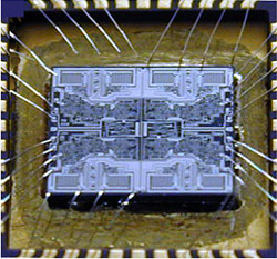
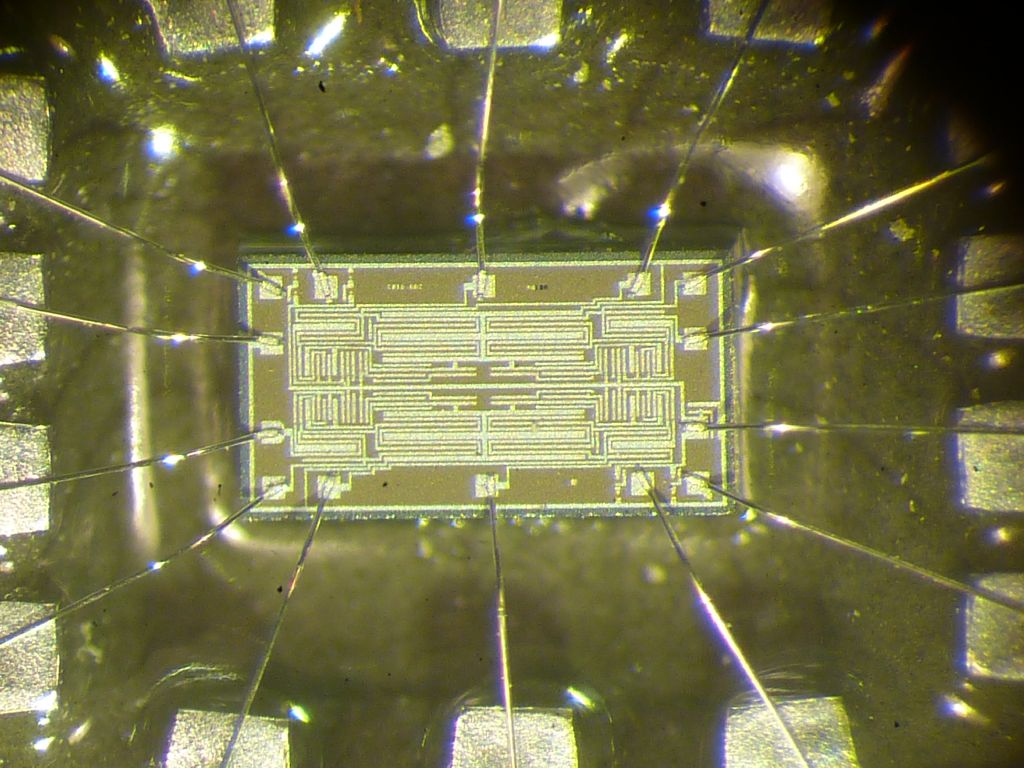
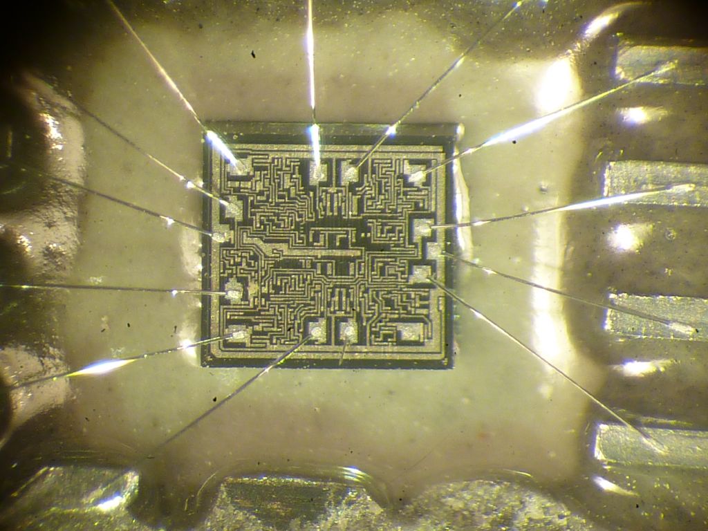
Attack Chip dsPIC33FJ256GP506A and compromise Microcontroller dsPIC33FJ256GP506 tamper resistance system, readout MCU software from dsPIC33FJ256 flash and eeprom memory
Attack Chip dsPIC33FJ256GP506A and compromise Microcontroller dsPIC33FJ256GP506 tamper resistance system, readout MCU software from dsPIC33FJ256 flash and eeprom memory;
Operating Conditions
· 3.0V to 3.6V, -40ºC to +150ºC, DC to 20 MIPS
· 3.0V to 3.6V, -40ºC to +125ºC, DC to 40 MIPS
Core: 16-bit dsPIC33F CPU
Timers/Output Compare/Input Capture
· Up to nine 16-bit timers/counters. Can pair up to make four 32-bit timers;
· Eight Output Compare modules configurable as timers/counters;
Code-efficient (C and Assembly) architecture
Two 40-bit wide accumulators
Single-cycle (MAC/MPY) with dual data fetch
Single-cycle mixed-sign MUL plus hardware divide
· Eight Input Capture modules
Communication Interfaces
· Two UART modules (10 Mbps)
– With support for LIN 2.0 protocols and IrDA®
· Two 4-wire SPI modules (15 Mbps)

dsPIC33FJ256GP506A یک کنترل کننده سیگنال دیجیتال با کارایی بالا از Microchip است که به طور گسترده در سیستم های صنعتی، خودروسازی و تعبیه شده استفاده می شود. با این حال، مکانیسمهای امنیتی آن میتواند از طریق تکنیکهای پیشرفتهای مانند تخلیه سیستمافزار، مهندسی معکوس و رمزگشایی به خطر بیفتد. این مقاله روش هایی برای کرک کردن، رمزگشایی و شبیه سازی برنامه ذخیره شده در حافظه فلش و EEPROM آن را بررسی می کند.
Clock Management
· Up to two I2C™ modules (up to 1 Mbaud) with ±2% internal oscillator
Programmable PLLs and oscillator clock sources
Fail-Safe Clock Monitor (FSCM)
Independent Watchdog Timer (WDT)
Fast wake-up and start-up
SMBus support
· Up to two Enhanced CAN (ECAN) modules (1 Mbaud) with 2.0B support
· Data Converter Interface (DCI) module with I2S codec support
Power Management
· Low-power management modes (Sleep, Idle, Doze)
· Integrated Power-on Reset and Brown-out Reset
· 2.1 mA/MHz dynamic current (typical)
· 50 μA IPD current (typical)
Advanced Analog Features
· Two ADC modules:
– Configurable as 10-bit, 1.1 Msps with four S&H or 12-bit, 500 ksps with one S&H
– 18 analog inputs on 64-pin devices and up to 32 analog inputs on 100-pin devices
· Flexible and independent ADC trigger sources
Input/Output
· Sink/Source up to 10 mA (pin specific) for standard VOH/VOL, up to 16 mA (pin specific) for non-standard VOH1
· 5V-tolerant pins
· Selectable open drain, pull-ups, and pull-downs
· Up to 5 mA overvoltage clamp current
· External interrupts on all I/O pins
Qualification and Class B Support
· AEC-Q100 REVG (Grade 1 -40ºC to +125ºC)
· AEC-Q100 REVG (Grade 0 -40ºC to +150ºC)
· Class B Safety Library, IEC 60730
Debugger Development Support
Packages
In-circuit and in-application programming
Two program and two complex data breakpoints
IEEE 1149.2-compatible (JTAG) boundary scan
Trace and run-time watch