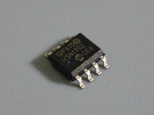
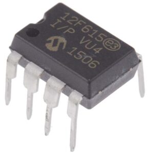
 Locked Microchip PIC12F615 Processor Data Restoration
Locked Microchip PIC12F615 Processor Data Restoration is a process to copy embedded firmware from original MCU PIC12F615 flash memory after break off the tamper resistance system of PIC12F615 locked microcontroller;

A Restauração de Dados do Processador PIC12F615 de Microchip Bloqueado é um processo para copiar o firmware incorporado da memória flash MCU PIC12F615 original após interromper o sistema de resistência à violação do microcontrolador bloqueado PIC12F615;
The Configuration bits can be programmed (read as ‘0’), or left unprogrammed (read as ‘1’), to select vari- ous device configurations. These bits are mapped starting at program memory location 300000h.
The user will note that address 300000h is beyond the user program memory space. In fact, it belongs to the configuration memory space (300000h-3FFFFFh), which can only be accessed using table reads and table writes.
Programming the Configuration registers is done in a manner similar to programming the Flash memory. The EECON1 register WR bit starts a self-timed write to the Configuration register. In normal operation mode, a TBLWT instruction, with the TBLPTR pointing to the Configuration register, sets up the address and the data for the Configuration register write.

Il ripristino dei dati del processore PIC12F615 del microchip bloccato è un processo per copiare il firmware incorporato dalla memoria flash originale dell’MCU PIC12F615 dopo aver interrotto il sistema di resistenza alle manomissioni del microcontrollore bloccato PIC12F615;
Setting the WR bit starts a long write to the Configuration register. The Configuration registers are written a byte at a time. To write or erase a configuration cell by breaking pic12f635 locked microprocessor fuse bit, a TBLWT instruction can write a ‘1’ or a ‘0’ into the cell. For additional details on Flash programming, refer to Section 6.5 “Writing to Flash Program Memory”.
bit 7 IESO: Internal External Switchover bit
1 = Internal External Switchover mode enabled
0 = Internal External Switchover mode disabled bit 6 FSCM: Fail-Safe Clock Monitor Enable bit
1 = Fail-Safe Clock Monitor enabled
0 = Fail-Safe Clock Monitor disabled
bit 5-4 Unimplemented: Read as ‘0’
bit 3-0 FOSC<3:0>: Oscillator Selection bits
11xx = External RC oscillator, CLKO function on RA6
1001 = Internal RC oscillator, CLKO function on RA6 and port function on RA7 1000 = Internal RC oscillator, port function on RA6 and port function on RA7 0111 = External RC oscillator, port function on RA6 when breaking pic12f609 locked mcu flash memory;
0110 = HS oscillator, PLL enabled (clock frequency = 4 x FOSC1)
0101 = EC oscillator, port function on RA6 0100 = EC oscillator, CLKO function on RA6 0010 = HS oscillator
0001 = XT oscillator
0000 = LP oscillator