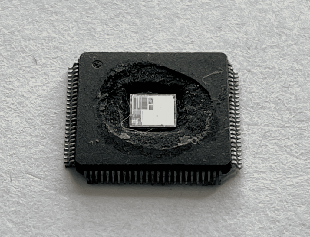
 Dump Renesas R5F212A7SDFA Protect MCU Flash Program
Dump Renesas R5F212A7SDFA Protect MCU Flash Program needs to know its internal structure and programming mechanism, extract its embedded firmware from R5F212A7SDFA microcontroller, and clone heximal file to new microprocessor R5F212A7SDFA;

R8C/Tiny series core
- Number of fundamental instructions: 89
- Minimum instruction execution time:
50 ns (f(XIN) = 20 MHz, VCC = 3.0 to 5.5 V)
100 ns (f(XIN) = 10 MHz, VCC = 2.7 to 5.5 V)
200 ns (f(XIN) = 5 MHz, VCC = 2.2 to 5.5 V)
- Multiplier: 16 bits × 16 bits ® 32 bits
- Multiply-accumulate instruction: 16 bits × 16 bits + 32 bits ® 32 bits
Operation mode: Single-chip mode (address space: 1 Mbyte)
3 circuits: XIN clock oscillation circuit (with on-chip feedback resistor) to breaking mcu R5F2L388 flash firmware,
On-chip oscillator (high-speed, low-speed)
(high-speed on-chip oscillator has a frequency adjustment function), XCIN clock oscillation circuit (32 kHz)
- Oscillation stop detection: XIN clock oscillation stop detection function
- Frequency divider circuit: Dividing selectable 1, 2, 4, 8, and 16
- Low power consumption modes:
Standard operating mode (high-speed clock, low-speed clock, high-speed on-chip oscillator, low-speed on-chip oscillator), wait mode, stop mode.

dump Renesas R5F212A7SDFA protegido MCU flash programa precisa conhecer sua estrutura interna e mecanismo de programação, extrair seu firmware incorporado do microcontrolador R5F212A7SDFA e clonar o arquivo heximal para o novo microprocessador R5F212A7SDFA
- External: 5 sources, Internal: 23 sources, Software: 4 sources
Priority levels: 7 levels
8 bits × 1 (with 8-bit prescaler)
Timer mode (period timer), pulse output mode (output level inverted every period), event counter mode, pulse width measurement mode, pulse period measurement mode.
8 bits × 1 (with 8-bit prescaler)
Timer mode (period timer), programmable waveform generation mode (PWM output), programmable one-shot generation mode, programmable wait one- shot generation mode