 Attack Microcomputer TMS320F243PGE Flash Code Reading Protection
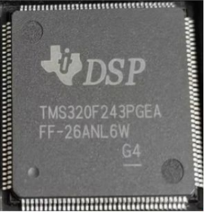
Attack Microcomputer TMS320F243PGE Flash Code Reading Protection needs to crack microcontroller tms320f243pge security fuse bit and then extract locked firmware from tms320f243pge flash memory;

Flash programming voltage pin and watchdog disable. This is the 5-V supply used for flash programming. Flash cannot be programmed if this pin is held at 0 V. This pin also works as a hardware watchdog disable, when VCCP/WDDIS = +5 V and bit 6 in WDCR is set to 1. Do not use a current-limiting resistor on this pin.
PLL oscillator input pin. Crystal input to PLL/clock source input to PLL. XTAL1/CLKIN is tied to one side of a reference crystal.
Crystal output. PLL oscillator output pin. XTAL2 is tied to one side of a reference crystal. This pin goes in the high-impedance state when EMU1/OFF is active low.
Clock output. This pin outputs either the CPU clock (CLKOUT) or the watchdog clock (WDCLK). The selection is made by the CLKSRC bit (bit 14) of the System Control and Status Register (SCSR) in the process of dsp microcontroller tms320f240pqe memory flash software recovery. This pin can be used as a GPIO if not used as a clock output pin.
External program space wait states. PSWS determines that between 0 to 7 wait states are applied to all reads and writes to off-chip program space address. The memory cycle can be further extended by using the READY signal. The READY signal does not override the wait states generated by PSWS. These bits are set to 1 (active) by reset (RS).

Angriffsmikrocomputer TMS320F243PGE Flash Code Leseschutz muss Mikrocontroller tms320f243pge Sicherheits Sicherungsbit knacken und dann gesperrte Firmware aus tms320f243pge Flash Speicher extrahieren;
External data space wait states. DSWS determines that between 0 to 7 wait states are applied to all reads and writes to off-chip data space. The memory cycle can be further extended by using the READY signal after decoding tms320f241fn dsp mcu program. The READY signal does not override the wait states generated by DSWS. These bits are set to 1 (active) by reset (RS).