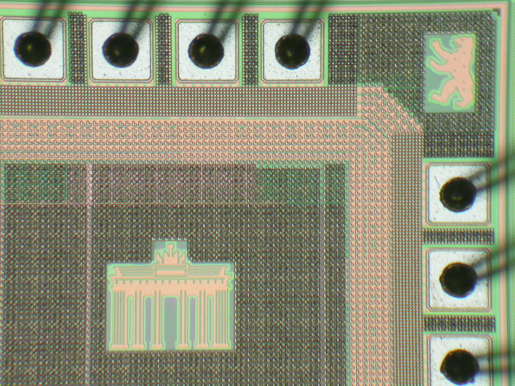
 Break Secured IC PIC16F716 Firmware
Break Secured IC PIC16F716 flash memory, cut off microcontroller PIC16F716 security fuse bit and extract firmware from MCU.

The PIC16F7X devices have a 13-bit program counter capable of addressing an 8K word x 14-bit program memory space. The PIC16F77/76 devices have 8K words of FLASH program memory and the PIC16F73/74 devices have 4K words when copy ic atmega8l heximal.
The program memory maps for PIC16F7X devices are shown in Figure 2-1. Accessing a location above the physically implemented address will cause a wrap around Firmware.
The RESET Vector is at 0000h and the Interrupt Vector is at 0004h. The Data Memory is partitioned into multiple banks, which contain the General Purpose Registers and the Special Function Registers.
Bits RP1 (STATUS<6>) and RP0 (STATUS<5>) are the bank select bits: Each bank extends up to 7Fh (128 bytes). The lower locations of each bank are reserved for the Special Function Registers after copy mcu pic32mx440f512 bin.
Above the Special Function Registers are General Purpose Registers, implemented as static RAM. All implemented banks contain Special Function Registers.
Some frequently used Special Function Registers from one bank may be mirrored in another bank for firmware reduction and quicker access. The register file (shown in Figure 2-2 and Figure 2-3) can be accessed either directly, or indirectly, through the File Select Register FSR Firmware.
The Special Function Registers are registers used by the CPU and peripheral modules for controlling the desired operation of the device. These registers are implemented as static RAM after IC breaking.
The Special Function Registers can be classified into two sets: core (CPU) and peripheral. Those registers associated with the core functions are described in detail in this section. Those related to the operation of the peripheral features are described in detail in the peripheral feature section.