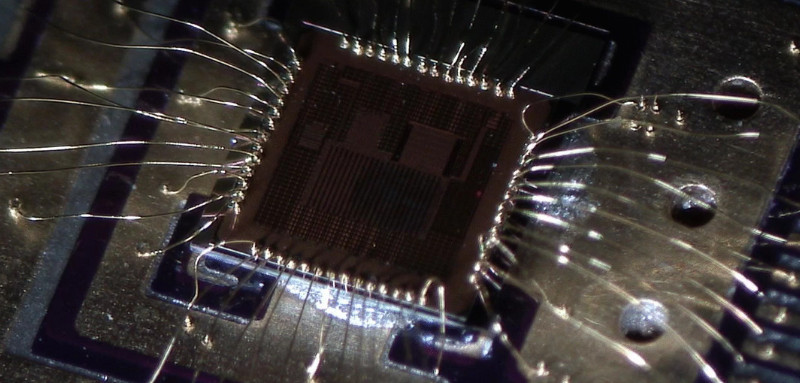
 STMicrocontroller STM8L052C6T6 Locked Flash Memory Decryption
STMicrocontroller STM8L052C6T6 Locked Flash Memory Decryption refers to unlock the fuse bit of stm8l052 by focus ion beam and extract source code from stm8l052 mcu flash memory.

The high-density and medium+ density STM8L15xx6/8x devices feature a nested vectored interrupt controller:
Nested interrupts with 3 software priority levels
32 interrupt vectors with hardware priority
Up to 40 external interrupt sources on 11 vectors
Trap and reset interrupts
The device requires a 1.65 V to 3.6 V operating supply voltage (VDD). The external power supply pins must be connected as follows:
VSS1, VDD1, VSS2, VDD2, VSS3, VDD3, VSS4, VDD4= 1.65 to 3.6 V: external power supply for I/Os and for the internal regulator. Provided externally through VDD pins, the corresponding ground pin is VSS. VSS1/VSS2/VSS3/VSS4 and VDD1/VDD2/VDD3/VDD4 must not be left unconnected by restoring microcontroller stm8s103k3 embedded flash memory.
VSSA, VDDA = 1.65 to 3.6 V: external power supplies for analog peripherals (minimum voltage to be applied to VDDA is 1.8 V when the ADC1 is used). VDDA and VSSA must be connected to VDD and VSS, respectively.
VREF+, VREF- (for ADC1): external reference voltage for ADC1. Must be provided externally through VREF+ and VREF- pin in order to reverse engineer microcontroller stm8s105k6 structure.
VREF+ (for DAC1/2): external voltage reference for DAC1 and DAC2 must be provided externally through VREF+.