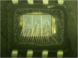
 Break IC PIC12CE519 Flash
The IC PIC12CE519 Flash memory, commonly used in embedded systems, plays a crucial role in storing firmware and other system data. However, for various reasons—such as debugging, security audits, or customization—accessing and modifying the data within this memory can be a challenge. At [Your Company Name], we offer specialized services to break the IC PIC12CE519 Flash, allowing you to unlock and modify the firmware to suit your needs.
PIC12CE519 Memoria flash, folosită în mod obișnuit în sistemele încorporate, joacă un rol crucial în stocarea firmware-ului și a altor date de sistem. Cu toate acestea, din diverse motive, cum ar fi depanare, audituri de securitate sau personalizare, accesarea și modificarea datelor din această memorie poate fi o provocare. La CECL, oferim servicii specializate pentru a sparge IC PIC12CE519 Flash, permițându-vă să deblocați și să modificați firmware-ul pentru a se potrivi nevoilor dumneavoastră.
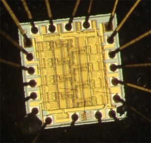
Our expert team uses advanced techniques to extract, disassemble, and analyze the data stored in the PIC12CE519 Flash. By employing specialized tools and custom scripts, we can access the firmware’s internal structure, providing you with a deeper understanding of its operation. Whether you need to identify vulnerabilities, reverse-engineer proprietary code, or recover lost data, we have the experience and tools to get the job done.
Our services are tailored to meet the unique needs of each client, ensuring precision, efficiency, and confidentiality. With our help, you’ll be able to unlock the full potential of your embedded systems and make informed decisions about security, optimization, or customization.
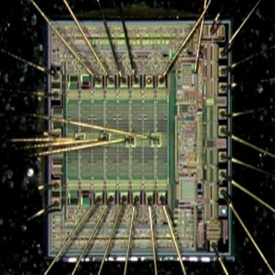
Unser Expertenteam verwendet fortschrittliche Techniken, um die im PIC12CE519-Flash gespeicherten Daten zu extrahieren, zu zerlegen und zu analysieren. Durch den Einsatz spezieller Tools und benutzerdefinierter Skripte können wir auf die interne Struktur der Firmware zugreifen und Ihnen so ein tieferes Verständnis ihrer Funktionsweise vermitteln. Ob Sie Schwachstellen identifizieren, proprietären Code zurückentwickeln oder verlorene Daten wiederherstellen müssen, wir haben die Erfahrung und die Tools, um die Arbeit zu erledigen.
Contact us today to learn more about how we can help you break the IC PIC12CE519 Flash and gain control of your embedded systems.
As with any other register, the I/O register can be written and read under program control when Break IC PIC12CE519 Flash. However, read instructions (e.g., MOVF GPIO,W) always read the I/O pins independent of the pin’s input/output modes. On RESET, all I/O ports are defined as input (inputs are at hi-impedance) since the I/O control registers are all set. See Section 7.0 for SCL and SDA description for PIC12CE5XX.
Serviciile noastre sunt adaptate pentru a răspunde nevoilor unice ale fiecărui client, asigurând precizie, eficiență și confidențialitate. Cu ajutorul nostru, veți putea debloca întregul potențial al sistemelor dvs. încorporate și veți putea lua decizii informate cu privire la securitate, optimizare sau personalizare.
GPIO is an 8-bit I/O register. Only the low order 6 bits are used (GP5:GP0). Bits 7 and 6 are unimplemented and read as ’0′s. Please note that GP3 is an input only pin. The configuration word can set several I/O’s to alternate functions. When acting as alternate functions the pins will read as ‘0’ during port read. Pins GP0, GP1, and GP3 can be configured with weak pull-ups and also with wake-up on change.
The wake-up on change and weak pull-up functions are not pin selectable. If pin 4 is configured as MCLR, weak pull-up is always on and wake-up on change for this pin is not enabled after Break Chip PIC12CE518 Binary.
The output driver control register is loaded with the contents of the W register by executing the TRIS instruction. A ’1′ from a TRIS register bit puts the corresponding output driver in a hi-impedance mode.
A ’0′ puts the contents of the output data latch on the selected pins, enabling the output buffer. The exceptions are GP3 which is input only and GP2 which may be controlled by Copy Chip PIC16F87 Code, The equivalent circuit for an I/O port pin is shown in below Figure.
Break IC PIC12CE519 Flash
All port pins, except GP3 which is input only, may be used for both input and output operations.
For input operations these ports are non-latching. Any input must be present until read by an input instruction (e.g., MOVF GPIO,W). The outputs are latched and remain unchanged until the output latch is rewritten. To use a port pin as output, the corresponding direction control bit in TRIS must be cleared (= 0). For use as an input, the corresponding TRIS bit must be set.
Any I/O pin (except GP3) can be programmed individually as input or output. Some instructions operate internally as read followed by write operations. The BCF and BSF instructions, for example, read the entire port into the CPU, execute the bit operation and re-write the result in order to Recover Microcontroller PIC16F71 Binary. Caution must be used when these instructions are applied to a port where one or more pins are used as input/outputs.
For example, a BSF operation on bit5 of GPIO will cause all eight bits of GPIO to be read into the CPU, bit5 to be set and the GPIO value to be written to the output latches. If another bit of GPIO is used as a bi- directional I/O pin (say bit0) and it is defined as an input at this time, the input signal present on the pin itself would be read into the CPU and rewritten to the data latch of this particular pin, overwriting the previous content.
As long as the pin stays in the input mode, no problem occurs. However, if bit0 is switched into output mode later on, the content of the data latch to facilitate the process of Crack MCU. The actual write to an I/O port happens at the end of may now be unknown.